Enabling the future of integrated photonics with thin-film lithium niobate
As PICs become ubiquitous, they are ushering in a revolution in computing, communication, and sensing. Quantum Computing Inc. (QCi) recently built an agile foundry dedicated to fabricating TFLN devices, providing unprecedented access to rapid prototyping and process-informed PIC design.
By Milan Begliarbekov, COO, and Pouya Dianat, CRO, Quantum Computing Inc.
Since the 1970s, Moore’s law has dominated the global technological landscape, with the number of transistors on a chip doubling about every two years. However, as physical limitations and rising costs become constraining factors, it is no longer practical to increase computing capacity by shrinking transistors. Furthermore, it has long been acknowledged that other physical phenomena underpinning the meteoric growth of CMOS are coming to an end.
Dennard scaling, for instance, described how the power density is roughly constant for a given die size, meaning that power usage and waste heat would not be increased by packing more, smaller transistors into the same area. Recent experiments, however, have shown that making transistors even smaller no longer reduces power consumption, but can in fact increase it due to effects like current leakage. Meanwhile, Amdahl’s law states that adding more processing cores can only reduce latency if the system is not bottlenecked by parts of a task that cannot run in parallel. This puts a limit on how much we can speed up processing simply by adding more components.
These seemingly disastrous obstacles to continued conventional CMOS scaling can only be overcome by a new paradigm of computing – a novel architecture that looks beyond the confines of von Neumann machines and embraces new materials to carry out computation. One solution looks towards integrated photonics, using light as the signal carrier and thus bypassing the physical limitations of electrical signals.
Using light opens up new possibilities for modulation, encoding, and data transmission by leveraging additional physical properties of photons. Unlike electrons travelling through copper wires, which usually only encode data in whether a current is flowing or not, light offers additional degrees of freedom; intensity, wavelength, polarisation, and even quantum properties like entanglement, can all carry information.
By harnessing these properties, we can significantly advance both classical and quantum computing, as well as usher in breakthroughs in AI, remote sensing, LiDAR, and biomedical sensing and imaging. Integrated photonics is rapidly building a new technological playground—one with the potential to revolutionise a wide range of fields through the development of next-generation photonic hardware.
The ultimate dream of integrated photonic engineers is to create a single chip that contains all four key elements necessary for computing with light: light sources, such as LEDs and lasers; passive components, which guide and route the light (such as waveguides and splitters); active components, which modulate or manipulate the light’s properties (such as phase, amplitude, or polarisation); and detectors, such as photodiodes and superconducting single-photon detectors, which capture and convert the light into electrical signals. While offering multiple functional advantages over traditional electronic integrated circuits, integrated photonics still benefits from using the same semiconductor fabrication technologies as those used in silicon-based microelectronics, to create PICs that manipulate light instead of, or in addition to, electrical signals.

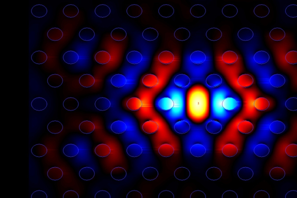
Figure 1. Key TFLN properties that enable QCi’s innovative technologies and products.
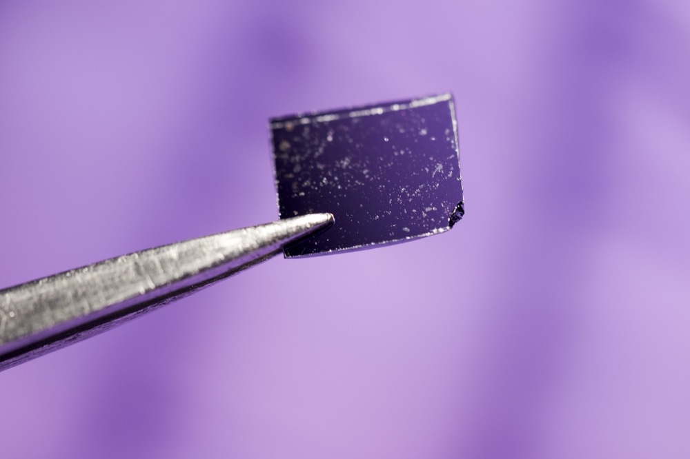
A key enabler of future photonic chips is thin-film lithium niobate (TFLN), a material that has gained significant traction in the telecommunications industry over the past decade due to advances in mechanical exfoliation and etching techniques. Lithium niobate itself is an established material with a proven 60-year history of utility as the active element in nonlinear optical components and in piezoelectric transducers, which transform mechanical energy into electrical energy and vice versa. But TFLN brings to the table even more exciting possibilities, since it overcomes the biggest limitation of the bulk material: the inability to tightly confine light.
TFLN PICs are the basis of optical engines in a new computing paradigm envisioned by Quantum Computing Inc. Currently, QCi has demonstrated this computing modality in our commercially available quantum optimisation machine, named Dirac-3, which is a unique quantum-hardware approach for tackling hard polynomial optimisation problems. Dirac-3 can solve problems with variables beyond binary (0,1), including non-negative integers, decimals, and sum-constrained continuous numbers (whose values must add up to a specific total).
The system consists of an optical-feedback loop that includes an optical amplifier, a photon-mode mixer/encoder, and a loss medium to implement both linear and nonlinear loss mechanisms. In particular, the core part of the system is a Mach-Zehnder mesh – an N x N grid of Mach-Zehnder interferometers – that requires high-performance modulators. Such components can be realised at scale and at a high level of functionality in a TFLN-based optical engine.
Why TFLN?
When selecting an ideal material for integrated photonics, PIC designers must consider three key factors: optical transparency, active device performance, and manufacturing compatibility.
First, the transparency window—the range of wavelengths a material can transmit with minimal absorption or scattering—is critical for passive components like waveguides that direct light across the chip. Ideally, this window should span from UV-VIS (400–750 nm) for remote sensing and imaging, to the O-band (1260–1360 nm) for short-reach, high-capacity telecom, and the C-band (1530–1565 nm) for long-haul fibre-optic communication.
Second, for high-performance active devices, the material should exhibit strong electro-optic and nonlinear optical properties. This includes a high Curie temperature, meaning the material will retain certain important properties and will still work well at high temperatures, the presence of free charge carriers to respond to electric fields, and a refractive index above 2.1 to enable light confinement. There should also be both high second-order (χ²) and third-order (χ³) nonlinear susceptibilities, meaning that certain interactions between light and the material depend on the square or cube of the light’s intensity.
Additionally, the electro-optic coefficient, which defines how much the material’s refractive index changes in the presence of an electric field, should be greater than 25 picometres per volt, to enable efficient periodic poling and modulation. Notably, such nonlinear properties are not equally achievable in silicon-based PICs as in TFLN.
Finally, from a manufacturing standpoint, the material must be compatible with existing high-volume production methodologies. This means it needs to possess thermal and mechanical stability, low insertion and propagation losses (< 0.1 dB per centimetre), and seamless integration with existing CMOS foundry processes.
Additionally, the material should have low switching voltages – the voltage change required for the optical modulator to switch the light signal between states – so that CMOS circuits can drive modulation directly. And on top of these qualities, the material should enable realistic paths to co-packaged optics and heterogeneous integration with other components and materials. For many materials that are being tested in academic labs, engineering them to fulfil these criteria remains a challenge.
Several emerging materials such as lithium niobate, lithium tantalate, and barium titanate are currently being considered for use in integrated photonics. However, among these, TFLN is the most mature, with a well-established supply chain and a strong track record of performance. TFLN is ideal for the datacom market since it enables high-speed modulation and dense signal encoding at a lower energy cost.
Specifically, TFLN devices have been shown to support ultra-fast switching speeds exceeding 100 GHz, low driving voltages (< 1 V to shift the light’s phase by half a wavelength), and large bandwidths. They are also CMOS-compatible, with exceptionally low insertion and operational losses (< 0.1 dB per centimetre). Compared to bulk lithium niobate, TFLN provides stronger light confinement, a high second-order (χ²) nonlinearity, appreciable third-order (χ³) effects, low propagation losses, and a large electro-optic response, supported by the presence of free charge carriers. These characteristics, summarised in Figure 1, make TFLN a highly versatile and high-performance platform, and an ideal choice of material for next-generation PICs.

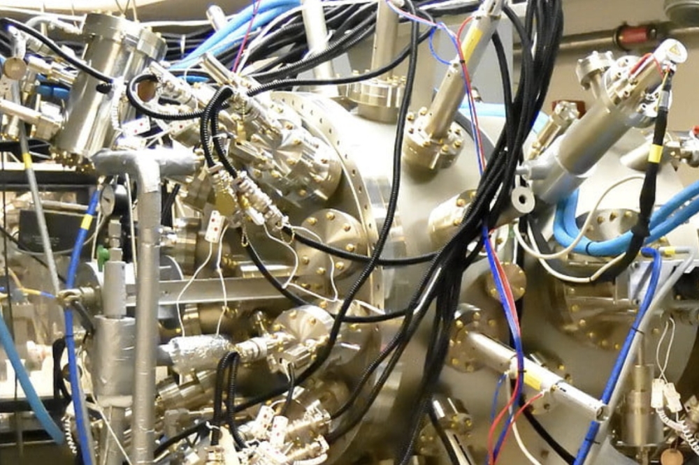
Figure 2. QCi’s core technologies use the quantum properties of light
and photonics to capture, compute, and communicate data. A dedicated
TFLN foundry provides a pathway to high-quality devices that optimise
performance metrics
with a compact footprint.
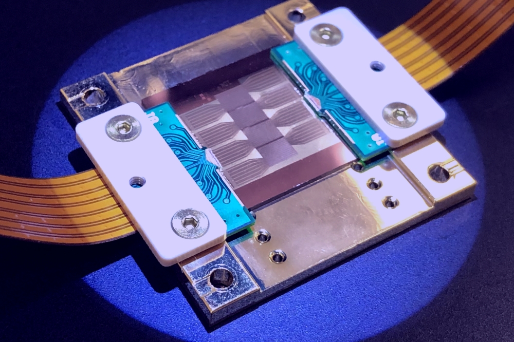
Electro-optic and acousto-optic modulators are two devices where TFLN offers immediate and significant advantages over bulk lithium niobate. Traditionally, making bulk LN modulators involves a process of diffusing titanium into the LN to create a contrast in refractive index and thereby form optical waveguides to direct the light. However, this approach results in poor light confinement, as the optical mode tends to leak into the surrounding material – ultimately limiting modulation speed. TFLN overcomes this problem by tightly confining the optical mode within nanophotonic waveguides, allowing for much higher switching speeds. The enhanced confinement not only boosts performance but also enables compact, chip-scale devices – often just a few millimetres in length – making TFLN modulators ideal for high-speed, high-density photonic integration.
The QCi Foundry
QCi is a vertically integrated company providing accessible and affordable quantum machines that leverage quantum optics and integrated photonics to either capture data, compute, or support communication.
The key enabling material in our devices is lithium niobate, but for the reasons described above it is also a limiting factor for both the device footprint and performance specifications. To support continued improvements to our technology, the bulky LN components need to be replaced with TFLN PICs, which improve upon the performance and, more importantly, the stability of bulk LN, while miniaturising the size of the photonic circuits.
The QCi Foundry, which recently opened in Tempe, Arizona, was built to strategically support the manufacturing of TFLN PICs for our quantum machines. Over the last 12 years, the academic community has demonstrated the exceptional performance of TFLN PIC components and gained expertise in high-quality fabrication (for example, producing smooth side walls in the material) while working at university or shared-user cleanrooms.
However, our quantum machines have such stringent requirements that a dedicated TFLN foundry, where each fabrication step can be tailored to and meticulously controlled for processing TFLN, is the only path forward in optimising our performance metrics.
From a broader perspective, there is a growing consensus that TFLN will be a key enabler of next-generation optical modules for datacentres—specifically 1.6T and 3.2T—driving demand for reliable and scalable fabrication facilities. As the photonics industry moves towards higher bandwidth and more compact solutions, a dedicated foundry service for TFLN could play a crucial role in accelerating this progress.
The QCi foundry’s main focus is on passive and active components—the parts that steer and shape the light on the chip. For more complex elements like lasers and detectors, viable solutions include co-packaging and heterogeneous integration – smart ways to combine different technologies into one system. Another important focus area for our foundry is creating periodically poled TFLN (PPLN) devices. While it is extremely challenging to manufacture PPLN devices with high yields, having access to high-quality PPLN components and PDKs is crucial for servicing the quantum markets. We view PPLN as the gateway to nonlinear integrated photonics which will enable chip-scale quantum computing.
Currently, the QCi foundry is in its first phase, with the initial goal of being able to rapidly prototype devices and bring them to medium-volume production. The toolset was selected to suit the needs of rapid prototyping for six-inch wafers, which allows the foundry to offer both custom and multi-project wafer (MPW) runs. The foundry offers a comprehensive suite of services including design and simulation, frontend and backend fabrication, as well as optical, DC and RF testing. All these in-house capabilities mean we can support our customers for the duration of their projects. Our process design kit, which currently includes standard component libraries, layout rules, and design rule check files, is now available on the GDSFactory+ platform to help streamline the PIC design process.

Figure 3. QCi’s foundry was constructed specifically for processing TFLN.
QCi’s long-term goal is to commercialise an entirely new paradigm of computing that looks beyond von Neumann architectures and embraces all-optical computing in both classical and later quantum variants. These technologies require nonlinear optical methods to carry out the computation, and TFLN is the ideal material to do this. Its robust nonlinear and electro-active properties, coupled with high transparency required for quantum devices, are essential for the next generation of computing and optical AI fabrics.
However, TFLN devices will need to meet highly rigorous specification demands to be suitable for quantum computing. This is why we have decided to build our own fab, where we can manufacture these devices to the highest standards. At this new facility, we will use the knowledge we gain from servicing the datacom and telecom industries as a stepping stone towards fully on-chip quantum devices.