Pure photonic CPUs: a future without electronics?
By using all-optical logic, memory, and multiplexing, Akhetonics is harnessing THz-frequency light on-chip, bypassing electronic speed limits and creating photonic processors that can advance AI inference, networking, and cryptography.
By Michael Kissner, CEO, Akhetonics
“What is the difference between electronic computing and photonic computing?” This is a question that we at Akhetonics often get asked. The quick answer is that one uses electrical signals and the other optical. Yet under the hood, both are just electromagnetic (EM) wave processors. At first glance, an electronic chip and a PIC even look alike, until you inspect them under a microscope and notice that photonic waveguides are much larger.
The difference really comes down to frequency. At low frequencies (Hz to MHz), the EM wave’s wavelength is enormous compared to chip features, so it makes sense to think of electrons shuttling through transistors instead of focusing on the wave. But once you move to the GHz domain, the wavelength is on the order of a millimetre – still much larger than most components, but it no longer covers the entire circuit in a single oscillation. Radio-frequency engineers must therefore think about guiding the wave as well, even if only in a fairly simple way.
When we increase the signal’s frequency by another factor of 1000, we reach the hundreds of THz, and it is all about the EM wave travelling through the system. The wavelength, now around a micrometre, has the same order of magnitude as the components needed to guide and process it on a chip. And this is precisely when we start calling it photonic – instead of electronic – processing.
In short: electronic integrated circuits cram billions of tiny transistors running at GHz speeds with long wavelengths. PICs have fewer components – tens of thousands – but operate at much higher frequencies and shorter wavelengths, allowing for blazing signal rates. It therefore makes sense that any THz CPU would need to be photonic in nature – and this is exactly what Akhetonics does.

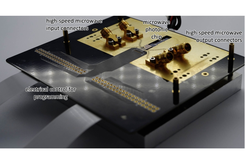
Figure 1. A pure photonic processor on a test bench, ready to process its first THz signals. (Image by Akhetonics)
But creating THz CPUs – or, as we like to call them, pure photonic CPUs – is far from trivial. An easy cop-out might be to keep traditional electronic processing in the loop and reserve photonics for communication. Luckily, there are indeed ways to move between frequency domains; photodiodes and modulators, for example, can convert signals from GHz to THz or vice versa. But any such conversion would instantly result in a bottleneck. If parts of the computer process in the photonic THz domain and parts in the electronic GHz domain, the total system will essentially still be limited to GHz, without a massive increase in parallelisation. To avoid this altogether, it seems obvious to ask: why not remain in the photonic THz domain while processing?
Of course, there is a reason why we do not already have THz CPUs. For electronics, the problem is not the transistor itself, as those have proven capable of handling low THz speeds. Rather, the issue is the large electric field coupling to everything nearby and causing a combination of resistance, capacitance, and inductance effects – collectively known as parasitics – which slow everything down. On the photonics side, since the EM wave is short enough to fit into a waveguide, we do not have parasitic interactions. But that also means it is hard to get light to interact at all.
Rethinking CPUs
To control one light beam with another like a transistor – a process called all-optical switching – we need to facilitate the interaction with a nonlinear optical medium. This has been possible for decades. In fact, the renowned physicist John von Neumann was granted the first patent for such a design in 1957 [1]. But so far there have been too many downsides to make it practical. Two of the most prominent ways to achieve all-optical switching are to use semiconductor optical amplifiers – which consume a great deal of power in their idle state – or highly nonlinear fibres – which require very long interaction lengths.
Nonetheless, both can be used for all-optical switching in a pure photonic CPU. The devices must simply meet four fundamental criteria. They must be cascadable, meaning that one device’s output can be fed as an input into another. They must also be fan-out, so that each device can drive the inputs of at least two others. Since we are computing with binary signals, we require logic-level restoration; the devices need to restore the highs and lows of the signal at each stage, so that the quality does not decline as the signal passes through the system. And finally, we need input-output isolation, meaning that the devices’ inputs and outputs are separated to avoid crosstalk.
These conditions are called Miller’s criteria for optical logic [2]. As long as they are satisfied, you can create any photonic binary logic circuit, including a CPU. However, using a slow, inefficient all-optical switch defeats the purpose of using light as the signal in the first place. To develop a high-performance all-optical switch, we need an optimal nonlinear optical material platform: one that offers strong nonlinear effects in compact structures, consumes little power, and can be integrated onto a PIC. No small feat, but two stand-out technologies are already on a path to commercialisation.
The first is a modified version of our trusted semiconductor optical amplifier in a III-V semiconductor platform, such as indium gallium arsenide phosphide (InGaAsP). While power hungry, they offer the most reliable operation of all methods of switching on a small scale. By carefully layering thin films of InGaAsP, engineers can finely tune how light interacts with the material to facilitate all-optical switching on a PIC. In our HAETAE project [3], together with the Aristotle University of Thessaloniki, imec, DGIST, and KAIST, we are exploring such a complete heterogeneous PIC platform for photonic computing.
The second promising technology harnesses 2D materials, which not only allow for THz speeds, but also extremely compact devices. Here our GATEPOST [4] and 2D Pilot Line [5] consortia seek to commercialise this novel material class for nonlinear photonics.
But even with these promising avenues for all-optical switching, a question remains. An electronic CPU has billions of transistors – how could we fit billions of micrometre- and millimetre-sized all-optical switches on a PIC? The answer is, we don’t. We are still years away from fitting millions of devices on a PIC, let alone billions. But we don’t necessarily need to. Instead, we must completely rethink our understanding of CPUs to design a photonic version.
Looking at electronic CPUs, they seemed to do just fine with thousands of transistors in the 70s and 80s. The MOS Technology 6502 microprocessor, introduced in 1975, has slightly more than 3,000 transistors and yet we still see it in use today, running fan favourite games, such as Super Mario Bros.

Figure 2. The GATEPOST project aims to use 2D materials to enable ultra-fast computing on a PIC. (Image by Akhetonics)
Intel’s x86-series debuted in 1978 with just shy of 30,000 transistors, running the first version of an instruction set that is still used by almost all desktop computers and laptops today.
We must recognise that the move from thousands to billions of transistors was for performance reasons, not fundamental capability. Then we can start using photonic computing’s inherent THz speeds, building architectures more akin to those of the 70s and seeing how they would compare to modern electronic CPUs.
As it turns out, running a photonic CPU with a mere thousand all-optical switches using a simple reduced instruction set computer (RISC) architecture, but at speeds a million times higher than its electronic predecessor, is very much within reach, at least on the processing side.
Memory and multiplexing
The problem now boils down to accessing memory, which is about 100 times slower than processing data. Modern electronic CPUs spend more than 99.9 percent of their transistor count not on actual computation tasks, but on working around this inherent memory bottleneck through tricks such as introducing cache, branch prediction, pipeline re-ordering, special instructions, and more. If photonic CPUs can’t solve this issue either, all our efforts would be futile.
The first component to look at is the interconnect between the CPU and memory. Linking the two electronically severely limits bandwidth; even advanced memory standards, such as DDR5, have not reached 10 giga transfers per second. And with round-trip latencies well beyond
10 nanoseconds on average, and peaking at 50-100 nanoseconds, this is simply not good enough for THz computing. It would mean, just as we see in electronics today, either a lot of idle time waiting for memory, or introducing all the complex optimisation structures we are trying to avoid.
Instead, photonic computing requires its own memory. But how do you slow light down to a standstill and call upon it at will? While that might not be feasible, we can use resonant structures to store an optical signal, while pumping or amplifying it, and manipulate the structure to store a new bit or release an old one. Integrated ring resonators, nanocavities, and even a flip-flop arrangement of all-optical switches can be used in this way. Related to this is delay-line memory, which was first used in electronic computing, and is used to manipulate optical signals in some contexts today.
But beyond storing light itself, we can also encode the signal in some other way, such as material transitions. Phase-change materials have been tried and proven as optical memories, for instance in DVDs or BluRays, and they are perfectly suited to integration on a PIC. The beauty of this solution is that the materials are non-volatile, so they can store data without a continuous power supply. In fact, reading them comes nearly for free, inducing minimal loss and, most importantly, happens instantaneously. Although we are not yet at the point of creating terabytes of volatile storage, researchers have gone beyond that on the read-only memory side, with projects such as 5D Optical Storage and Project Silica demonstrating petabyte storage capabilities.
As well as solving the issue of memory, we also need to consider how we can achieve efficient processing with far fewer components than an electronic CPU. Here, photonics has a superpower: its potential for multiplexing. Two, ten, or even hundreds of optical signals of different wavelengths can travel inside a single waveguide without affecting each other significantly. This capability has driven an industry-wide adoption of optical networking, enabling the transmission of terabits of data per second over a single strand of fibre.
But this multiplexing does not have to be restricted to optical communication; we can use it for photonic computing as well, effectively making a multi-core processor out of a single physical core. Furthermore, since photonics does not induce parasitics, we can also use dense time multiplexing within the processor or introduce multiplexing based on phase and polarisation.
The parallelisation options are almost limitless, with one goal: minimise the number of physical components and instead add more multiplexing for performance. Quality over quantity.

Figure 3. PICs enable the integration of a variety of optical materials
for computing and memory, such as phase change materials (PCM) seen here
covering a waveguide. (Image by Akhetonics)
Processors for purposes
With photonic all-optical switching, all-optical memory, and multiplexing strategies in place, what can we build? We can create logic circuits that integrate on the order of 10,000 all-optical switches, and we have a limited amount of volatile optical memory and plenty of read-only memory. This may not be a great starting point to run an operating system like Linux, but perhaps L4.
Interestingly, it’s very similar to what a GPU looks like. GPUs have numerous smaller cores, called shader units, that run lock-step in groups, performing the same operation on different bits of data. This massively parallel computation enables fast, efficient processing. But it also means GPUs work best if they treat most memory as read-only. Otherwise, any write-induced race condition, in which multiple cores try to write to the same piece of memory at the same time, would kill performance.
And for the purpose for which they were designed, this is exactly how GPUs are used. 3D renderings or complex graphics games treat their assets as static resources that do not change in-memory, but rather are “shaded”. Through computational steps, the static asset is fed through a pipeline of shaders and transformed and animated for a specific situation in a game, or setting in a 3D render. Incidentally, these shaders are often computing how light interacts with its environment. It would seem only fitting to actually use light to do those calculations in a pure photonic processor.
But we aren’t focusing on running games – at least not yet. A very similar application is AI inference. Current AI hardware treats the model as largely static once trained, allowing it to reside in read-only memory. Neural network layers, in many ways, resemble shaders, and could be similarly handled in our photonic CPU. While the majority of processing is linear algebra, we must not underestimate the amount of branching (“if-then”-statements) and nonlinear arithmetic such as activation functions. These demands are addressed by the design of our pure photonic arithmetic and logic unit within the CPU.
Of course, we will always need some working memory. Luckily, we have our photonic memory available, and this is truly what sets the binary photonic CPU apart from its analogue cousin. Analogue computing is great for mathematics, but struggles with branching operations and has essentially no solution for memory. It therefore requires interactions with electronic processors, which kill its performance and efficiency by constantly moving between the electronic and photonic domains. This is why almost all companies in the analogue photonic computing space, such as Lightmatter, Ayar Labs, and Celestial AI, have decided to move to interconnecting electronic chips using their technology as a photonic interposer instead.
Another advantage of pure photonic computing chips is that their relatively large structures make them compatible with mature semiconductor nodes using 90 nm, 130 nm, and even 250 nm processes. This could open the door to production at a wide range of foundries globally, potentially shifting the balance from a TSMC-Intel-Samsung-centric landscape for high-performance fabrication to a much more open environment, significantly reducing supply chain risks. What’s more, these mature processes are typically more cost-effective and environmentally friendly than leading-edge processes for advanced electronics.
But even if our pure photonic computing approach solves a lot of issues that have plagued electronic or electro-optical hybrid computers, it is not ideal for every use case. AI training, for example, which requires terabytes of volatile storage, will simply not benefit from photonic computing in the near future. Photonic computing must pick its early priorities, and the most promising are centred around AI inference, graphics processing, networking, cryptography, and real-time systems. This is where the pure photonic approach really shines, although it will likely be another two or three years before we see the first commercial devices in the wild.
So no, pure photonic computing does not mean a future without electronics. Even if we could run everything using light, different applications would still need to process different frequencies throughout the EM spectrum. From Hz to THz, the specific use case dictates which processing capabilities we need. That said, where high performance is key, we are sure to see much more photonics on the horizon.