Enabling secure quantum communications with photonic components and integrated circuits

Fraunhofer HHI is advancing quantum key distribution systems by developing photonic components such as single-photon detectors and transmitters based on InP, and creating hybrid PICs that can generate photon pairs and control their polarisation states.
By Nino Walenta, Patrick Runge and Moritz Kleinert, Fraunhofer HHI
In an era marked by growing concerns over cybersecurity and data privacy, quantum communication is emerging as a promising solution for secure information exchange. Although classical encryption methods have so far been robust, they are increasingly vulnerable to advances in computing – especially the anticipated capabilities of quantum computers.
Quantum communication systems aim to ensure information-theoretic security – meaning it cannot be broken even with unlimited computational resources and time. These systems leverage principles such as quantum entanglement, which links pairs of particles, and the no-cloning theorem, which prevents quantum information from being perfectly copied. Such principles can be seen at work in quantum key distribution (QKD), a well-known cryptographic task that enables two parties to share encryption keys with security rooted in the laws of physics.
However, realising practical quantum networks requires more than just theoretical foundations; it depends critically on scalable, stable, and high-performance photonic systems. Photons are ideal quantum information carriers, since they do not interact much with the environment and they are compatible with existing optical fibre networks. To support quantum communication, advanced photonic components such as low-loss waveguides, integrated sources of entangled photons, and high-speed single-photon detectors are vital.
Moreover, PICs enable the miniaturisation and mass production of quantum devices, paving the way for cost-effective deployment. This synergy between quantum principles and photonic technologies will form the backbone of next-generation communication infrastructure.
Figure 1. SPAD module with the key performance parameters measured at
1550 nm wavelength for room temperature and internally TEC cooled
operation.
Photonic components
One of the main challenges in the quantum industry is detecting photons in the short-wave infrared (SWIR) wavelength range (1000-1600 nm). For shorter wavelengths up to 900 nm, single-photon avalanche diodes (SPADs) fabricated on silicon material platforms work well. However, when targeting the use of low-loss single-mode fibres for QKD applications, detectors must operate at telecom-wavelengths from the O- to L-band. In this case, indium phosphide (InP) is the material platform of choice.
For quantum applications requiring detectors that can pick up just a few photons, there are photodiodes available with high detection efficiencies of 99 percent [1]. This is sufficient for certain applications, such as those using squeezed light. However, other applications require yet higher-sensitivity detectors that can even catch individual photons with high accuracy.
To achieve this performance, systems need to incorporate either internal amplification to boost the detection signal, or superconductivity to reduce background noise from electrical resistance. A drawback of the latter is its need for cryogenic cooling, which is impractical for most non-academic settings.
SPADs are a preferred choice for industrial applications, thanks to their compact size, high reliability, and low power consumption. However, these devices suffer from dark counts, meaning they occasionally generate a false detection signal when no photon is present. Since dark count rates (DCR) can significantly impact the system performance, for example by reducing the signal-to-noise ratio and decreasing the secret key rate, the system design must consider this parameter. However, moderate cooling with a thermoelectric cooler (TEC) reduces the DCR significantly, meaning that the SPAD’s packaging becomes as important as the design of the chip itself.
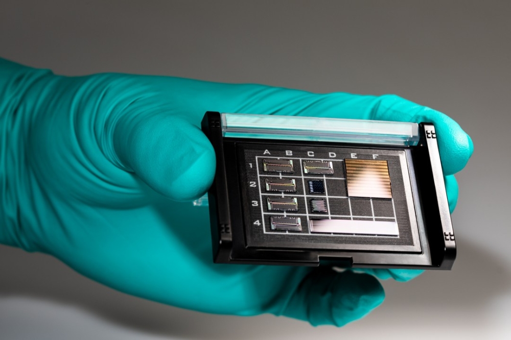
Figure 1 shows a fibre-coupled SPAD module with a system application-oriented housing (fibre in-plane with printed circuit board (PCB)) and its measurement results [2]. Besides the excellent photon detection efficiency (PDE) and DCR, the module performs well on several other characteristics. It has an afterpulsing probability – or likelihood of generating a false secondary signal shortly after a genuine detection – of under 0.5 percent. This is measured at a hold-off time of 10 µs, during which it is intentionally switched off to “reset” after a detection.
Additionally, the timing jitter, or uncertainty about precisely when each photon triggers the detection signal, is just 162 picoseconds.
The SPAD module also has a compact footprint of less than a thumbnail and includes a TEC that can cool the device to 70 degrees C below the temperature of its environment. With this cooling, the module can achieve a DCR of 1500 counts per second and 25 percent PDE, which represents state-of-the-art performance at 1550 nm. Besides the SPAD design itself, the fabrication technology, including the high-quality epitaxial growth of the semiconductor layer stack, contributes to its excellent performance.
Since the SPAD operates by triggering an electrical current when it detects a photon, it also needs an inbuilt process to stop this current, “resetting” it so it is ready for the next photon. This is called quenching and there are multiple ways of achieving it.
Typically, QKD systems use one of two techniques: high-speed gating or free-running passive quenching. In the former setup, a voltage source sets the SPAD above the breakdown voltage – the threshold value at which the voltage is high enough to set the photodetector to single-photon detection mode. The voltage source repeatedly drops below this value and returns to it at a defined time interval, continually turning the SPAD off and resetting it.
Meanwhile, the other quenching technique sets the SPAD into a free-running passive quenching mode, in which the voltage source remains constantly above the breakdown voltage. If a detection event generates a photocurrent, an internal resistor reduces the voltage, which drops across the SPAD, until the current stops. The voltage then recovers so the SPAD can detect another photon. SPADs with internal resistors are called negative feedback avalanche diodes.
Figure 2. Thin-film filter as a polarising beam splitter/combiner (left) and as a pump light suppression filter (right).
On the transmitter side, InP-based PICs are excellent candidates for QKD signal generation, since they enable monolithic integration of lasers and electro-absorption modulators. Moreover, InP PICs are already a mature technology, thanks to well established component manufacturing for the telecom industry. With a few minor design changes, telecom PICs can be readily adapted for QKD transmitters.
Since QKD systems rely on single-photon interactions, the PIC design needs to include variable optical attenuation, to reduce the emitted light intensity. Additionally, to provide the random numbers that QKD systems use to ensure secure encryption, the design incorporates quantum random number generators built to introduce non-deterministic processes such as laser beating or laser switching.
Researchers have already demonstrated high-performance transmitter QKD components on InP PICs, showing the potential of this approach [3] [4]. As a cost-efficient low entry level for InP PIC development, engineers can use multi-project wafers to get experience with PIC design and characterisation.
Figure 3. Polarisation-encoded BB84 DV-QKD transmitter (left) with resulting polarisation states (right).
Hybrid PICs
While monolithic integration of photonic functionalities in a single material platform, namely InP, is advantageous for some quantum applications, others have stringent specifications that cannot all be fulfilled by a single material. Often these specifications set conditions on various characteristics, from waveguide losses and spectral operating range to the handling of the polarisation and the use of nonlinear processes.
This is where hybrid integration of chips from two or more material platforms comes into play. Through hybrid integration, engineers can combine low-loss passive waveguide platforms, such as silicon nitride or polymers, with a broad spectral transparency from the visible to the infrared, and active semiconductor components individually optimised for their respective functionality.
Over the past decade, Fraunhofer HHI has developed its hybrid photonic integration platform PolyBoard, which uses passive polymers as a waveguiding platform. In contrast to dielectric or crystalline materials, which are deposited by epitaxial methods, PolyBoard is made of polymer films, which are fabricated by subsequent spin coating and curing steps. This allows for great flexibility in the layer stacks, so each device can be tailored to its target application and wavelength. The material is easily structured by dry etching, allowing for deeply etched slots and grooves on the chip.
The precise etching in the PolyBoard platform enables the efficient on-chip integration of micro-optical elements, such as thin-film filters (TFFs), for example. TFFs consist of a micrometre-thin polymer film and a dielectric layer stack deposited on top, and they offer a solution to a pressing issue in photonic integration for quantum communications: efficient filtering and light conditioning.
When TFFs are inserted into etched slots on the chip perpendicularly to the waveguide layer, it is the dielectric layer stack, not the waveguides, that determines the filter characteristic. This approach allows PICs to benefit from highly efficient dielectric filters, which are already employed in free-space optics.
Figure 2 shows two examples of TFFs used in quantum communications applications. On the left is the transmission spectrum of a TFF used as a polarising beam splitter/combiner. The right-hand side presents a filter for the suppression of pump light for the nonlinear generation of photon pairs. Here, we observe an extinction of 85 dB of the 785 nm pump light. As well as being highly efficient, the TFF-based filtering has the advantage that it does not require phase or temperature stabilisation, making it ideally suited for applications outside of laboratory settings.
Figure 4. Photon pair source module relying on the micro-optical bench in the PolyBoard platform.
In the context of quantum communications, being able to efficiently handle the polarisation of light is especially important for QKD transmitters that encode qubits in this property. Figure 3 shows such a transmitter realised in the PolyBoard platform. It uses four individual tuneable lasers, emitting transverse electric (TE)-polarised pulses in the C band. The two inner waveguides pass through a TFF serving as a half-wave plate, which rotates the polarisation from TE to transverse magnetic (TM).
Subsequently, these TM-carrying waveguides are recombined with the outer TE-carrying waveguides by TFFs acting as polarising beam combiners. One of these arms is then rotated once more by another TFF half-wave plate. This results in one arm carrying light in a state of diagonal polarisation, and the other carrying light in a state of antidiagonal polarisation. Finally, the two waveguides are combined and fed into a variable optical attenuator, which attenuates the pulses down to the single-photon level.
By selecting the input laser from the laser array and carefully controlling its light pulses, we can choose the polarisation state of the output, whether it is in the horizontal/vertical basis or the diagonal/antidiagonal basis. In this way, the TFFs allow for passive on-chip handling of the polarisation to create qubits with a maximum deviation of less than 6 degrees from the ideal polarisation states. This fulfils the requirement of QKD implementation to be able to send photons in specific polarisation states.
While many QKD transmitters can use attenuated lasers as photon sources, some quantum applications require true single photons or photon pairs. One common way of generating single photons and photon pairs is via spontaneous parametric down conversion. In this process, a high-energy, short-wavelength photon is directed into a nonlinear crystal, stimulating the emission of two lower-energy, longer-wavelength photons.
The main challenges in miniaturising these photon sources are the difficulty of integrating nonlinear crystals onto a PIC and the on-chip suppression of the pump light. The PolyBoard platform offers a way of overcoming both obstacles. The module shown in Figure 4 is an integrated photon pair source, in which a nonlinear periodically poled KTP crystal from Raicol Crystals is integrated into an on-chip free-space section. In this section, gradient refractive index (GRIN) lenses form a collimated beam profile, enabling the integration of micro-optical elements that are on the order of a few millimetres long.
The 785 nm pump light is coupled into the chip through a polarisation-maintaining fibre. Once in the chip, the pump light causes the integrated crystal to generate photon pairs, which are collected by a second GRIN lens and coupled into the on-chip waveguides.
After the crystal, a chip-integrated TFF as presented on the right-hand side of Figure 2 suppresses the 785 nm pump light by 85 dB, so that only the 1550 nm photons are emitted at the chip output. Subsequently, the photons are separated by polarisation with a TFF polarising beam splitter, and the single photons are finally coupled into single-mode fibres where they are readily available for transmission.
The two hybrid PICs presented here for use in quantum communications exemplify the versatility of hybrid photonic integration, especially for emerging applications.
System integration
The integration of high-performance photonic components in PICs is pivotal in transitioning quantum communication from laboratory research to real-world applications. These technologies enable the development of compact, scalable, and robust quantum communication systems, facilitating the deployment of QKD in practical settings.
Fraunhofer HHI has developed a high-speed QKD system that illustrates this integration. The system is based on the BB84 QKD protocol, and encodes the data in the photons according to the time interval they arrive in and their phase relative to a reference (time-phase encoding). It also uses a single decoy-state method, sending additional non-qubit photons to increase security, operating at a qubit frequency of 625 MHz.
The system features instant optical switching and routing capabilities for the quantum channel, without the need for a separate dedicated channel to establish synchronisation between the sender and receiver.
Its design allows for fast automatic startup and continuous operation over both fibre and free-space optical links, and is compatible with various single-photon detectors, enhancing its adaptability to different operational environments.
A quantum random number generator serves as the primary source of randomness, ensuring the unpredictability of the generated keys, and thus the security of the encryption.
The synergy between advanced photonic components, PICs, and standardised protocols underscores the feasibility of establishing secure quantum networks.
By leveraging these technologies, we can implement QKD systems that are not only secure, but also practical for widespread adoption, marking a significant step towards realising quantum communication networks.


