NIST Chip Lights Up Optical Neural Network Demo
Researchers at the National Institute of Standards and Technology (NIST) have made a silicon chip that distributes optical signals precisely across a miniature brain-like grid, showcasing a potential new design for neural networks.
The human brain has billions of neurons (nerve cells), each with thousands of connections to other neurons. Many computing research projects aim to emulate the brain by creating circuits of artificial neural networks. But conventional electronics, including the electrical wiring of semiconductor circuits, often impedes the extremely complex routing required for useful neural networks.
The NIST team proposes to use light instead of electricity as a signaling medium. Neural networks already have demonstrated remarkable power in solving complex problems, including rapid pattern recognition and data analysis. The use of light would eliminate interference due to electrical charge, and the signals would travel faster and farther.
"Light's advantages could improve the performance of neural nets for scientific data analysis such as searches for Earth-like planets and quantum information science, and accelerate the development of highly intuitive control systems for autonomous vehicles," NIST physicist Jeff Chiles said.
A conventional computer processes information through algorithms, or human-coded rules. By contrast, a neural network relies on a network of connections among processing elements, or neurons, which can be trained to recognize certain patterns of stimuli. A neural or neuromorphic computer would consist of a large, complex system of neural networks.
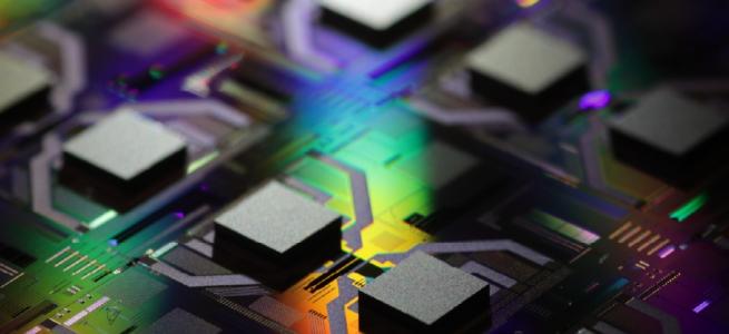
Described in a new paper, the NIST chip overcomes a major challenge to the use of light signals by vertically stacking two layers of photonic waveguides"”structures that confine light into narrow lines for routing optical signals, much as wires route electrical signals. This three-dimensional (3D) design enables complex routing schemes, which are necessary to mimic neural systems. Furthermore, this design can easily be extended to incorporate additional waveguiding layers when needed for more complex networks.
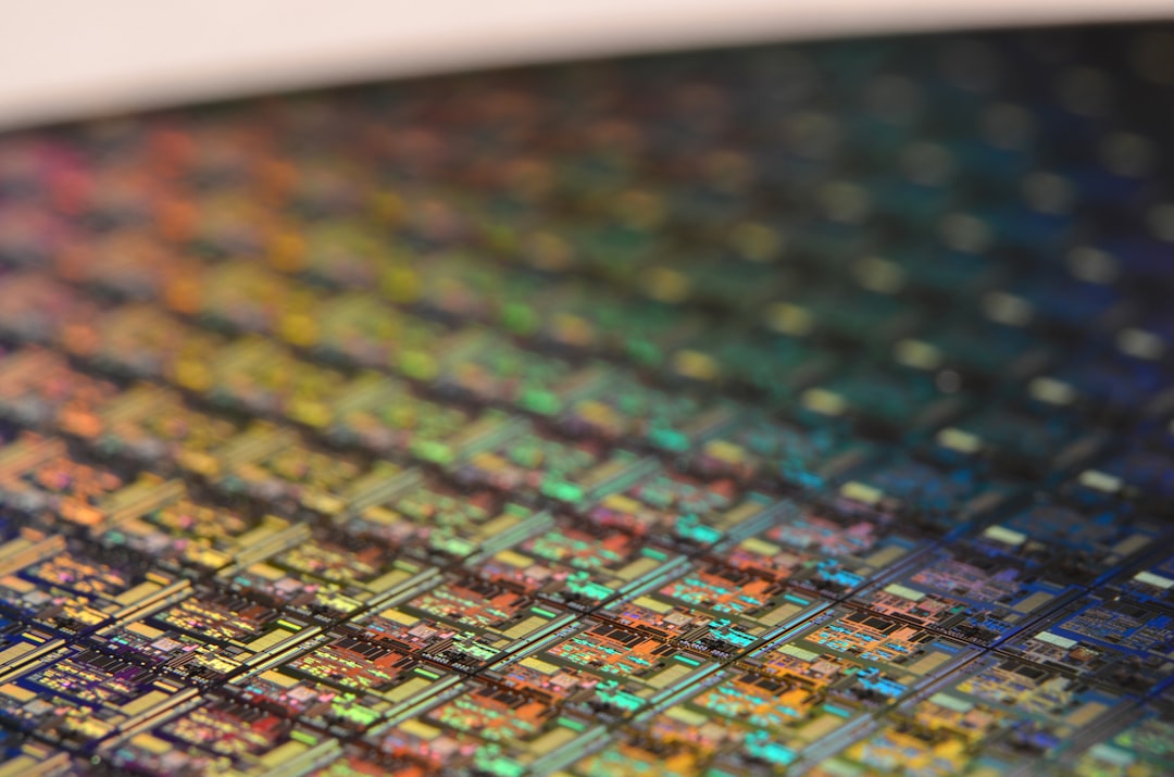
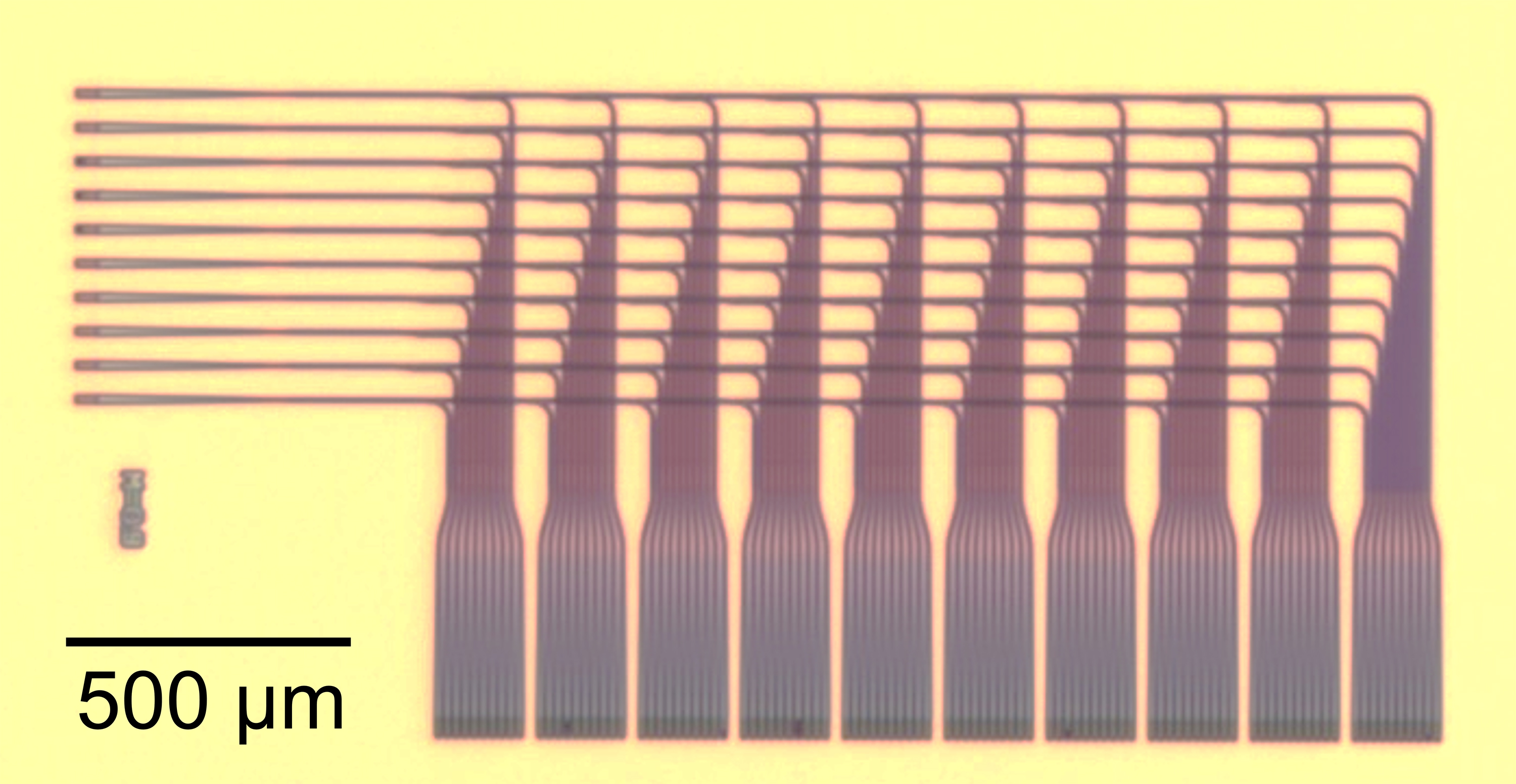
The stacked waveguides form a three-dimensional grid with 10 inputs or "upstream" neurons each connecting to 10 outputs or "downstream" neurons, for a total of 100 receivers. Fabricated on a silicon wafer, the waveguides are made of silicon nitride and are each 800 nanometers (nm) wide and 400 nm thick. Researchers created software to automatically generate signal routing, with adjustable levels of connectivity between the neurons.
Laser light was directed into the chip through an optical fiber. The goal was to route each input to every output group, following a selected distribution pattern for light intensity or power. Power levels represent the pattern and degree of connectivity in the circuit. The authors demonstrated two schemes for controlling output intensity: uniform (each output receives the same power) and a "bell curve" distribution (in which middle neurons receive the most power, while peripheral neurons receive less).
To evaluate the results, researchers made images of the output signals. All signals were focused through a microscope lens onto a semiconductor sensor and processed into image frames. This method allows many devices to be analyzed at the same time with high precision. The output was highly uniform, with low error rates, confirming precise power distribution.
"We've really done two things here," Chiles said. "We've begun to use the third dimension to enable more optical connectivity, and we've developed a new measurement technique to rapidly characterize many devices in a photonic system. Both advances are crucial as we begin to scale up to massive optoelectronic neural systems."
Paper: J. Chiles, S.M. Buckley, S.W. Nam, R.P. Mirin and J. M. Shainline. Published July 26, 2018. Design, fabrication and metrology of 10x100 multi-planar integrated photonic routing manifolds for neural networks. APL Photonics. doi:10.1063/1.5039641