International team makes stretchy photonic devices
Light-based devices could be used as biomedical sensors or as flexible connectors for electronics.
Researchers at MIT and several other institutions have developed a method for making photonic devices that can bend and stretch without damage. They think the devices could find uses in cables to connect computing devices, or in diagnostic and monitoring systems that could be attached to the skin or implanted in the body, flexing easily with the natural tissue.
The findings, which involve the use of chalcogenide glass, are described in an upcoming paper by MIT's Juejun Hu and more than a dozen other researchers at the University of Texas, Xiamen University and Chongqing University in China, Universite Paris-Sud in France, the University of Southampton in the UK, and the University of Central Florida. The paper will be published in Light: Science and Applications.
Hu, who is the MIT Merton C. Flemings Associate Professor of Materials Science and Engineering, says that many people are interested in the possibility of optical technologies that can stretch and bend, especially for applications such as skin-mounted monitoring devices that could directly sense optical signals. Such devices might, for example, simultaneously detect heart rate, blood oxygen levels, and even blood pressure.
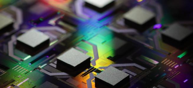
Most current photonics devices are fabricated from rigid materials on rigid substrates, Hu says, and thus have an "inherent mismatch" for applications that "should be soft like human skin." But most soft materials, including most polymers, have a low refractive index, which leads to a poor ability to confine a light beam.
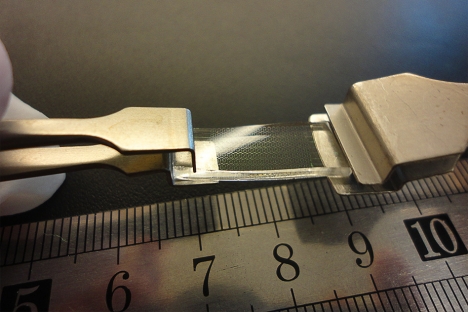
Instead of using such flexible materials, Hu and his team formed the stiff material "” in this case a thin layer of a type of glass called chalcogenide - into a spring-like coil. The architecture of this glass coil allows it to stretch and bend freely while maintaining its desirable optical properties.
"You end up with something as flexible as rubber, that can bend and stretch, and still has a high refractive index and is very transparent," Hu says. Tests have shown that such spring-like configurations, made directly on a polymer substrate, can undergo thousands of stretching cycles with no detectable degradation in their optical performance. The team produced a variety of photonic components, interconnected by the flexible, spring-like waveguides, all in an epoxy resin matrix, which was made stiffer near the optical components and more flexible around the waveguides.
Other kinds of stretchable photonics have been made by embedding nanorods of a stiffer material in a polymer base, but those require extra manufacturing steps and are not compatible with existing photonic systems, Hu says.
Such flexible, stretchable photonic circuits could also be useful for applications where the devices need to conform to the uneven surfaces of some other material, such as in strain gauges. Optics technology is very sensitive to strain, according to Hu, and could detect deformations of less than one-hundredth of 1 percent.
This research is still in early stages; Hu's team has demonstrated only single devices at a time thus far. "For it to be useful, we have to demonstrate all the components integrated on a single device," he says. Work is ongoing to develop the technology to that point so that it could be commercially applied, which Hu says could take another two to three years.
In another paper published last week in Nature Photonics, Hu and his collaborators have also developed a new way of integrating layers of photonics, made of chalcogenide glass and 2D materials such as graphene, with conventional semiconductor photonic circuitry.
Existing methods for integrating such materials require them to be made on one surface and then peeled off and transferred to the semiconductor wafer, which adds significant complexity to the process. Instead, the new process allows the layers to be fabricated directly on the semiconductor surface, at room temperature, allowing for simplified fabrication and more precise alignment.
The process can also make use of the chalcogenide material as a "passivation layer," to protect 2D materials from degradation caused by ambient moisture, and as a way to control the optoelectronic characteristics of 2D materials. The method is generic and could be extended to other emerging 2D materials besides graphene, to expand and expedite their integration with photonic circuitry, Hu says.
The research team also included MIT Professor Jing Kong, MIT postdocs Lan Li and Hongtao Lin, and others at the University of Texas, Xiamen University and Chongqing University in China, Universite Paris-Sud in France, the University of Southampton in the UK, and the University of Central Florida.
The work was supported by the US National Science Foundation and made use of the MIT Microsystems Technology Laboratories.