Technical Insight
Fabrication challenges for enabling metropolitan WDM network technologies (Cover Story)
Issues relating to the fabrication of echelle grating demultiplexers based on indium phosphide a building-block for next generation integrated optical components are described by Bedwyr Humphreys and Emil Koteles of MetroPhotonics Inc.
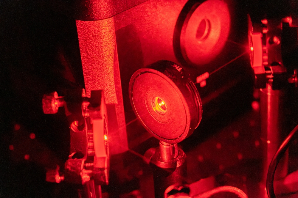
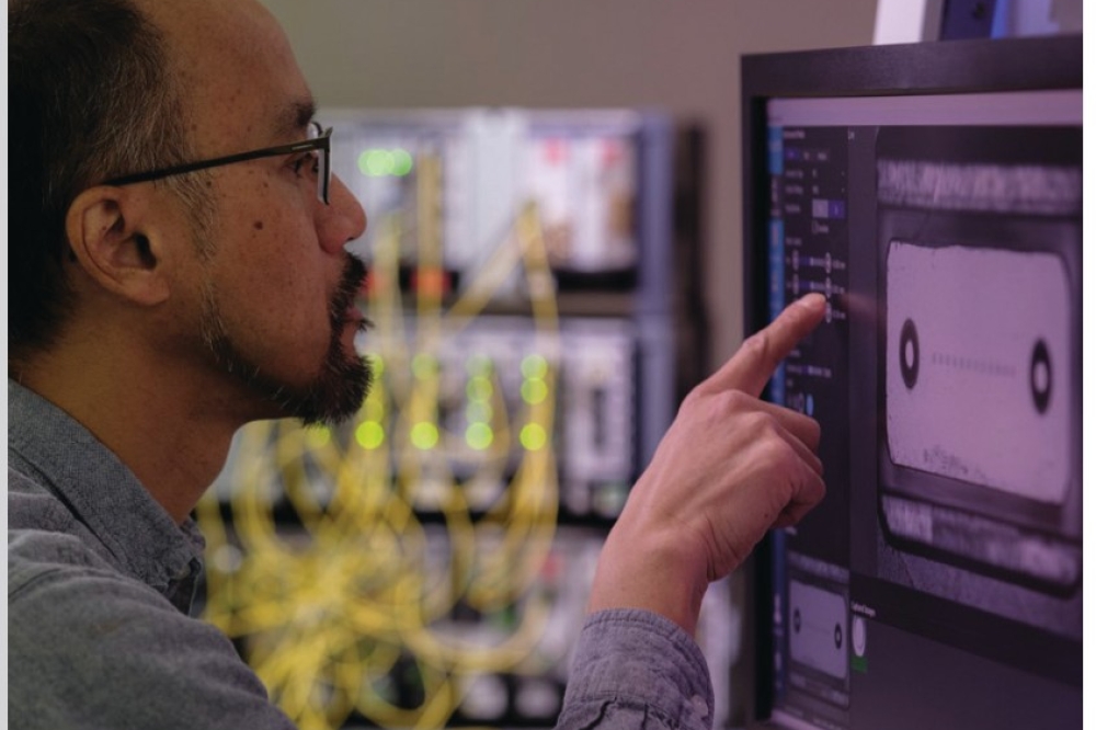
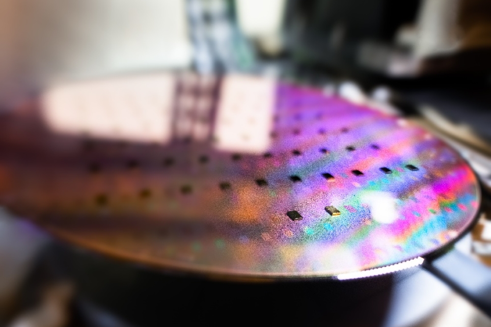
The Internet s future depends on migrating the large bandwidth that is present in optical backbones of telecommunications networks around the world to homes and businesses. Long haul WDM components, the savior of the backbone, are just too expensive for metropolitan markets. The key enabler is cost. Recent advances in monolithically integrated (de)multiplexers (planar waveguide etched grating devices) and a novel, elegant technique for flattening DWDM channel spectra without increasing crosstalk promise a cost-effective solution. Inexpensive WDM components, made possible by photolithographic processing techniques and increased manufacturing tolerances, will help unleash the full potential of the Internet to all. Until recently, WDM signal processing (generation, detection, multiplexing, demultiplexing, etc) has been accomplished using discrete optical components. These perform well but their fabrication is labor intensive and so they are expensive to manufacture. It is universally believed that the next generation of optical components will be based on integration technology. The planar waveguide is the technology of choice for monolithic photonic integrated circuits (PICs) since such circuits can be easily fabricated using standard semiconductor photolithographic processing techniques. Two-dimensional (planar) optical wave-guides can be fabricated using a variety of materials, although glass and semiconductors are the most common. By increasing the refractive index slightly (for example through the use of ridges see ), light can be directed, at will, in the plane (Koteles). Some two decades ago, planar waveguides were first proposed for demultiplexing (and multiplexing) WDM wavelengths. The first "spectrometer-on-a-chip" was based on echelle grating technology, itself over a hundred years old. schematically illustrates a typical etched grating demultiplexer (DEMUX) based on InP waveguides. Light from a singlemode fiber is coupled into the edge of the chip at the input waveguide. The light follows the guide to its end, where it begins to expand in the 2-D plane until it reaches the grating, which is etched through the waveguide. The grating reflects and disperses the light and focuses it onto an arc located near the input waveguide. There, a series of output waveguides collects the dispersed light and transports it to the edge of the chip, where it is either detected or collected by other optical fibers. The fabrication of the grating required a deep vertical etch with smooth sidewalls, but unfortunately such capability was not available at the time. For these reasons, Meint Smit of Delft University in the Netherlands and others (Smit) developed an alternative technology, the phasar or arrayed waveguide (AWG) DEMUX (see ). This device solved these issues but had other drawbacks (see "Echelle grating and AWG demultiplexers"). Fabrication challenges Deep vertical etching of semiconductor material has come a long way in recent years with much attention being paid to materials such as InP and GaAs. In particular, many studies looked at the possibility of using dry etching for on-chip facet fabrication in long-wavelength InP-based devices. Early studies used reactive ion etching (RIE) to achieve the anisotropy required, and although successful in principle, many of the processes could not be implemented for manufacturing due to very low etch rates and excessive damage. The development of the inductively coupled plasma (ICP) source for use in semiconductor processing proved to be a turning point, providing higher etch rates, improved anisotropy and the potential for lower damage processing. Many of the factors considered for the fabrication of etched facets also apply to the fabrication of echelle gratings. These factors are primarily confined to photolithography and etching, with key requirements on certain process parameters. Photolithography requirements Correct selection of photolithography tools can mean the difference between success and failure, hence a thorough understanding and analysis of key device parameters and how they may be affected by the photolithography process is essential. Photomask fabrication There are a number of choices to be made regarding the type of photomask to be used, e.g. binary, phase shifted, laser write, in addition to the choice between 1:1 or 5:1 pattern transfer. The photomask fabrication method employed and the choice of materials determines the accuracy of the pattern on the mask or reticle as well as the quality, e.g. feature resolution (rounding errors) and stitching errors. Rounding errors result from the finite step size of the mask machine, whereas stitching errors occur when small write fields are "stitched" together to form a large element, e.g. the array of waveguides in the AWG. Rounding errors The impact of rounding errors on device performance is to produce a more or less constant noise background (non-adjacent crosstalk) that decreases as rounding errors are reduced. In addition to photomask rounding errors, rounding at sharp feature edges can occur during pattern transfer due to nonlinear distortions caused by optical diffraction and resist process effects. Causes include reticle pattern fidelity (as discussed), optical proximity effects, and loading effects during resist and etch processing. Stitching errors When translated onto the device, stitching errors on the photomask produce mode structure on the sides of the main channel spectra that die away in intensity as a function of distance. These "ghosts" can be eliminated by using only one field (no stitching) or by increasing the field size. It is possible for an etched grating DEMUX in InP to be written in a single field since the grating size is comparable to the largest field size (1 mm) in state-of-the-art e-beam writers. In addition to photomask considerations, the more typical manufacturing elements to consider include photoresist thickness and uniformity, and exposure dose reproducibility and uniformity, all of which need careful control using statistical process control (SPC) techniques. For example, photoresist thickness and uniformity can drift out of specification if environmental controls for temperature and humidity fluctuate beyond a few degrees (see "Materials for Planar Waveguides"). Dry etch requirements One of the major requirements for the fabrication of echelle gratings is a vertical etch profile. Typically, the tolerance on the profile angle for achieving a working device with acceptable losses is less than 0.5. Achieving this specification depends on a number of parameters, both lithography- and etch-related. These include the following. Vertical etch-mask profile A sloped etch-mask profile is more likely to result in a sloped feature etch, especially when the mask selectivity is low (see ). High mask selectivity The greater the selectivity between the mask and the etch layer, the greater the likelihood of a vertical etch profile regardless of the mask profile. Infinite selectivity processes are almost impossible to develop, hence a combination of vertical profile and high selectivity is the optimum practical solution (see ). Low mask damage Minimal damage to the mask edge is required to prevent loss of mask integrity at the mask/semiconductor interface. Low mask damage also reduces the likelihood of vertical striations being transferred from the mask edge into the etched feature. Facet striations in all optical devices should be kept to a minimum. High anisotropy Zero undercutting of the mask maintains precise feature pattern transfer into the etched layer. The etched profile should remain vertical throughout with no bowing of the profile. High etch rate Echelle gratings or etched facets usually require a relatively deep etch, thus a high etch rate is desirable to maintain a reasonable wafer throughput. Hardware configuration Having defined the process requirements and characteristics, the next step is to determine the hardware configuration best suited to achieve the requirements. The types of system currently on offer for plasma etching include parallel plate RIE, magnetically enhanced RIE (MERIE), M0RI (m=0 resonant induction) and ICP. The suitability to the task can be determined by assessment of the critical operational parameters and how these in turn affect the defined process requirements and characteristics. The critical operational parameters in plasma etching are process pressure, ion energy, ion density and process chemistry. Low pressure processing (