Wafer-level nanoimprint technology for innovative packaging

The need for high-speed data transfers with low-power consumption and low latency in data centers, telecom networks, sensors and emerging applications in advanced computing for artificial intelligence (AI) is growing exponentially. More than ever, we rely on these applications to ensure a safer and more productive world. All across these markets, silicon photonics (SiPh) play a key role in enabling ultra-high bandwidth performance. As a result, it is more important than ever to develop solutions that can cost-effectively scale up the production of silicon photonics.
By Andrea Kneidinger, EV Group
While the wafer manufacturing capabilities for SiPh have matured through the use of standard semiconductor mass production processes and existing infrastructure, packaging solutions for SiPh remain a key bottleneck to mass commercialization.
Production capabilities for SiPh are still behind and lack scalability compared to wafer fabrication. The main limiting factor is the fiber to chip assembly, where companies today often rely on very complex solutions; for example, direct fiber bonding on chip with adhesive through active alignment or high-precision tools. These factors limit the wider deployment of SiPh. To solve this challenge, EV Group (EVG) teamed up with Teramount to develop optical microstructures using a simple, reliable and cost-effective wafer-level replication process that enables the production and scaling up of complex structures to high volumes. This replication process, known as nanoimprint lithography (NIL), helps to simplify, miniaturize and standardize the optical interface to bridge the gap in SiPh packaging toward wafer-level high-volume manufacturing (HVM).
NIL overview
NIL is a precise replication technique that has shown to be ideally suited to facilitate the patterning of microstructures with challenging geometries, required for emerging devices and applications across the photonics market. This technology is very flexible and can produce a wide range of shapes and structures, such as mirrors, prisms, spheric and aspheric lenses, micro lens arrays as well as various types of diffractive structures. Supported dimensions can be freeform and range from single nanometer resolution up to millimeter lateral extent. These 3D structures are replicated in a single step, which is ideally suited for the photonics industry, where light matter interaction relies largely on shape and geometry.
A further key asset of NIL is the straightforward transfer of these complex and high-precision structures to HVM as hundreds or thousands of structures can be replicated with high fidelity over a large area in a single step. Overall, wafer-level NIL represents an efficient and low-cost non-conventional lithography method capable of replicating complex micro- and nano-scale structures, particularly wafer-level optics (WLO).
Step and Repeat Mastering: scaling NIL from single die to fully populated master
Step-and-repeat (S&R) NIL is a key enabling technique for manufacturing wafer-level micro- or nanostructures because it bridges a crucial gap between die-level designs and wafer-level production. In particular, it allows the scaling of structures that were previously prototyped on areas measuring in the square-millimeter range to fill full 200-mm or 300-mm wafers. The main challenge with S&R NIL is that the quality of the initial master stamp defines the success of subsequent production, so the quality of the single-die master must be preserved. Therefore, it is necessary to take a master mold of a single die — written with either an electron beam, direct laser writing, or two-photon polymerization — and replicate it exactly hundreds or even thousands of times to produce full-area masters for 200-mm or even 300-mm wafer production lines (see Figure 1).
To address this need, EVG has developed the EVG770 S&R NIL system, which enables precise replication of micro- and nano-patterns for large-area master stamp fabrication used in HVM. It dispenses the resist, aligns the structures, imprints accordingly and demolds in a fully automated procedure. To support the most advanced mastering requirements, the S&R system includes full process control, with precision alignment within 250 nm, and is capable of positioning every structure next to alignment patterns. All process steps — from dispensing, imprint, curing, and demolding — must also be performed precisely and monitored within a single environment to allow optimal feedback control.
This not only avoids the impact of external sources such as airborne particles or temperature changes that can lead to imperfections, but it also enables the creation of both a wafer-level master with optimal quality and exact replicas of every single die that can then be applied to wafer-level manufacturing.
With every replication step — from single die to S&R master to working stamp and final imprint — some changes in pattern dimensions are inevitable, due to shrinkage of the polymers caused by crosslinking during the UV curing process. These changes are predictable, some steps can even compensate for each other, and the deviations from the original design are very repeatable for a given set of materials. Thus, compensation can be calculated into the master design. Flexible fabrication methods, such as 2GL (two photon greyscale lithography) or e-beam, support such design changes as well as short iteration times.
Figure 1: EVG’s NIL process and scaling know how: from single die, via Step and Repeat (S&R), to fully populated master and high-volume manufacturing.
Wafer-level NIL for high-volume manufacturing
The S&R mastering process is followed by wafer-level NIL replication, which is performed on the EVG7300. This process consists of two steps, both of which are carried out on the same system (Figure 2). First, the S&R master is replicated to fabricate a working stamp. This step is particularly useful because it minimizes wear of the expensive masters and reduces the risk of introducing defects. Defective working stamps can be replaced quickly and at low cost, which can be particularly advantageous during high-volume production runs.
Figure 2: Schematic of a NIL process, consisting of two steps: working stamp fabrication and imprint. Both steps are carried out in the same tool.
To ensure defect-free working stamp fabrication, the initial master is coated with an anti-sticking layer applied by spin coating. Next, the working stamp material is coated directly on the master, also by a spin coating process, using an EVG120 spin/spray coating system. Next, the transparent backplane is attached on the coated master. The working stamp polymer is then cured using an UV LED light source, and finally demolded from the master.
After the working stamp is produced, the actual imprinting process on the device substrate is performed. This involves applying a dedicated material on the substrate using the same spin coating process used for the working stamp fabrication.
Next, the working stamp and the substrate with the dispensed material are brought into contact with each other. As was the case with the working stamp fabrication process, this step is followed by UV curing and demolding, resulting in multiple imprints with the final devices on the substrate. The working stamp can then be reused for multiple imprints, increasing NIL process efficiency. This method of reusing working stamps has been proven already for HVM applications.
The NIL process has long proven its high repeatability in high-volume production for optical sensors and is now being leveraged for replicating complex optical structures for silicon photonic packaging. It offers significant yield and cost advantages for these structures compared to conventional manufacturing methods, such as diamond drilling, laser direct writing and electron-beam writing, which are difficult to scale up to larger substrates and limited in their throughput. Incorporating the NIL process enables the use of best-performing dies and the ability to efficiently bring these high-quality patterns into production lines. In particular, the precise alignment to the underneath optical structures on the photonic chip is crucial for the excellent coupling performance needed within the SiPh packaging devices. NIL can also produce complex structures, which typically are not possible to produce through standard CMOS processes, such as optical coupling elements of mirrors and lenses with sharp edges, curved surfaces or structures with high and low aspects ratios. The ability of NIL to provide high pattern fidelity, repeatability and accurate placement of optical elements on SiPh wafers plays a key role in shifting the typical fiber packaging complexity from the assembly domain to the wafer manufacturing domain.
Teramount collaboration
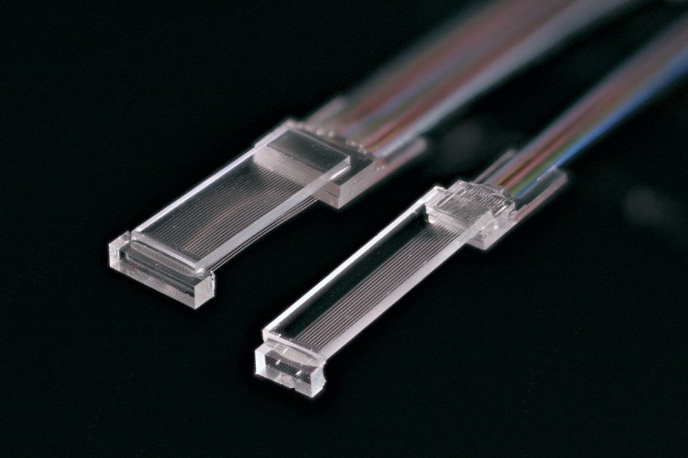
EVG’s collaboration with Teramount illustrates how NIL can help enable a paradigm shift in SiPh packaging. Teramount implements its PhotonicPlug and PhotonicBump wafer-level optical elements through the use of NIL – aligning photonic packaging with standard semiconductor manufacturing and packaging flow. NIL provides an ideal platform for post-processing of silicon photonic wafers for the photonic “bumping” process to be performed either at semiconductor foundries or at outsourced semiconductor assembly and test (OSAT) facilities.
Figure 3: a) PhotonicBump NIL imprint on a SiPh wafer next to multi-channel photonic integrated circuit waveguides; Figure 3:b) Close-up image shows PhotonicBump elements including beam deflection and beam expansion mirrors.
NIL has been used to imprint PhotonicBumps on eight-inch SiPh wafers for performing wafer-level optical coupling elements from and to waveguides of photonic integrated circuits. Figure 3a shows PhotonicBumps imprinted next to a multi-channel SiPh chip, and Figure 3b shows a close-up of a PhotonicBump imprinted in close proximity to a single waveguide channel. PhotonicBump incorporates a deflector mirror imprinted inside a 20-micron cavity depth and a second element of lensed mirror. The deflector mirror performs vertical beam deflection to enable wide-band surface coupling as a replacement for the complicated side-coupling geometry, which is typically used in silicon photonics packaging. The lensed mirror is used for beam expansion for establishing a self-aligning optical scheme[1] and for generating large assembly tolerances when combined with PhotonicPlug fiber connectors shown in Figure 4.
Figure 4: Left) a diagram of PhotonicPlug fiber connector assembled on a “bumped” SiPh chip. Figure right) PhotonicPlug optical elements including single-mode fibers, deflector mirror and beam expansion mirror. PhotonicPlug optics form a self-aligning optical scheme when combined with PhotonicBump optics.
Figure 5 shows the optical coupling performance of PhotonicPlug when packaged with a bumped SiPh chip. Figure 5a shows XY tolerance map and Figure 5b shows x-cross section with a large assembly tolerance of >±30µm/0.5dB and a total insertion loss of 1dB from fiber to waveguide. Such superior performance demonstrates PhotonicPlug and PhotonicBump capabilities as well as the advantages of NIL technology to perform accurate placement of wafer-level optical elements.
Figure 5a) Measured XY map of PhotonicPlug assembly tolerances when coupling to SiPh chip. Figure 5b) X-cross section of PhotonicPlug assembly tolerance presenting >±30 µm/0.5dB and a total insertion loss of 1dB from fiber to waveguide.
Working in conjunction with Teramount’s PhotonicBump packaging technology, NIL is making wafer-scale packaging possible in the photonics industry, which could have a profound impact on lowering packaging and overall product costs. Whereas packaging is still a relatively small (but growing) share of overall CMOS production costs, it presents the majority of overall cost in photonics manufacturing, which still relies on single device packaging schemes. Wafer-level integrated photonics, enabled by NIL and PhotonicBump packaging, has the potential to flip this equation. Through this combination of NIL process and innovative optical elements, the bottleneck in SiPh packaging is being shifted to the optical design rather than fiber assembly tolerance.
NILPhotonics Competence Center: A flexible cooperation mode
As part of the joint-collaboration between EVG and Teramount, EVG provided NIL process development and prototyping services through its NILPhotonics Competence Center, as well as expertise in both CMOS and photonics manufacturing, to assist Teramount in accelerating the development and productization of its PhotonicPlug technology.
EVG’s NILPhotonics Competence Center provides an open access innovation incubator for customers and partners across the NIL supply chain to collaborate to shorten development cycles and time to market for innovative photonic devices and applications.
The center is highly flexible and adapts to the varied needs of customers while ensuring the highest level of IP protection for every aspect of development. The cleanroom is designed to meet the most stringent customer requirements and allows for virtual line concepts where wafers are reintroduced into customer fabs for further processing.
Acknowlegdements and referencesThe author wishes to thank Hesham Taha of Teramount for his assistance with the development of this article.
[1] “Photonic plug for scalable silicon photonics packaging”, A. Israel et al. Proc. SPIE 11286, Optical Interconnects XX, 1128607 (28 February 2020); doi: 10.1117/12.2543490


