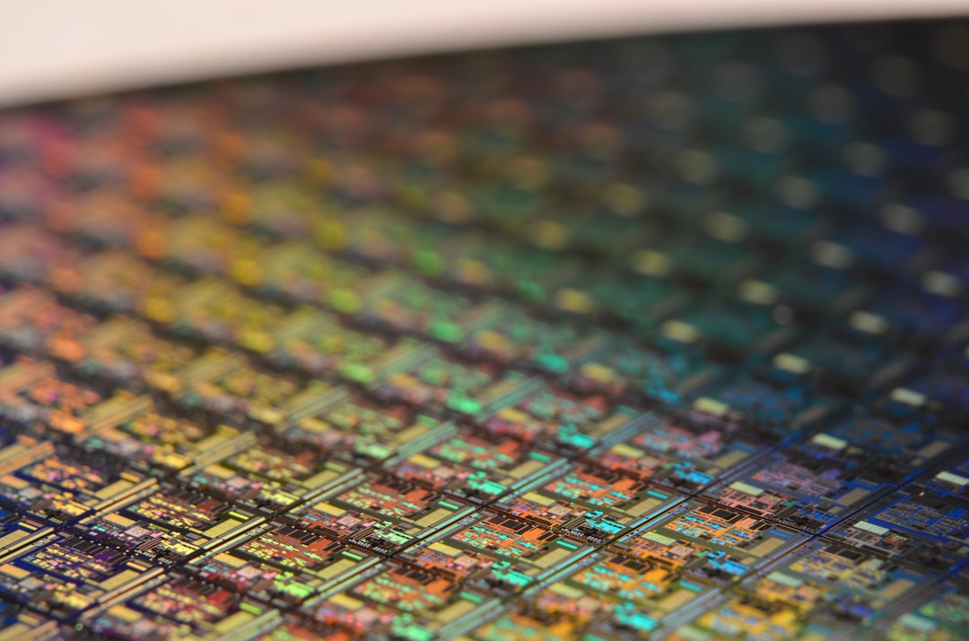
Big step forward in silicon integration
Until the last couple of years, research into silicon photonics had been moving at snail s pace. Now things seem to be happening at breakneck speed. "Silicon photonics is on fire!" is how Graham Reed, head of electronic engineering at the University of Surrey, UK, puts it.
"Just look at the number of Nature papers in the past two years," he said. "There is a daily increase in the number of groups and companies in this field."
One of those companies is Intel, the biggest player in silicon electronics bar none. But it is also at the forefront of the emerging silicon photonics research field. In September, it revealed details of an electrically pumped hybrid III-V/silicon laser, developed in collaboration with researchers at the University of California, Santa Barbara (UCSB). While many key optical functions have been demonstrated on a silicon platform, finding a suitable light-emitting source has posed the biggest problem – until now, it appears.
According to Intel, the breakthrough addresses one of the last major barriers to producing silicon photonics for use inside and around future computers and data center architectures. In essence, that means using components compatible with volume silicon manufacturing methods to generate, amplify, route, modulate and detect light in very high speed terabit optical interconnects of a suitable size for a high-performance computer.
Reed, whose credentials include initiating the field of silicon optical integrated circuits in the UK, concurs: "This device has a lot of potential" he said. "There s no doubt that it s certainly a very significant piece of the puzzle. While it s not truly a silicon laser, it s probably the next best thing".
The flurry of silicon photonics papers appearing in the leading science journals over the past couple of years suggests that with the fundamental building blocks in place, integration of these various components in an optical system has now become the major challenge.
For example, electro-optic modulators are one of these key building blocks. Earlier this year a Danish team published details in Nature of just such a device. Using a silicon nitride layer to compressively strain the active layer of silicon, Rune Jacobsen from the Technical University of Denmark and colleagues discovered that this strain induces a linear electro-optic effect that can modulate light at high speeds. In theory, it could be used instead of an electronic "bus" to transport data in computer architectures.
Unlike some other approaches to optical modulators based on silicon, the device proposed by the Jacobsen team is not limited by any charge mobility or carrier recombination effects. They argue that this could be a critical advantage when it comes to commercial deployment of silicon-based photonics because these effects could limit modulation speeds.
Despite the apparently different material platforms that the Danish team s modulator and Intel s hybrid silicon laser are based upon, Reed believes that these two devices could, in theory, function together as part of an optical system. "Most of the parts that are emerging are compatible at a high level because they are almost all based on a silicon-on-insulator (SOI) platform," he said.
Intel s hybrid laser is made by fusing together a AlGaInAs/InP quantum well structure and a silicon strip waveguide. That waveguide is first formed on the surface of an undoped SOI substrate. The "special sauce" that allows the laser to function is the way that the silicon waveguide and the active AlGaInAs layers bond.
Both surfaces are treated in an oxygen plasma reactive ion etch chamber, pressed together and annealed. The materials couple so well that the III-V and silicon elements each form a critical part of the laser structure, with the silicon waveguide fundamental to the lasing action. The degree of alignment between the two types of material does not require a particularly high level of precision. John Bowers from UCSB has been leading the research: "All of the optical mode confinement – in the laser, in subsequent modulators, in output waveguides and in a fiber holder – is determined by the same CMOS lithography step," he explained.
According to Graham Reed, the complexities of integrating lasers, modulators and detectors will always throw up issues of compatibility, particularly when it comes to processing optical and electronic parts in the same layer of material. For high-end applications capable of 40 Gbit/s communications, it will also be necessary to develop another part – a silicon-based optical isolator – that can be easily integrated into a circuit.
These high modulation frequencies will have to be achieved in Intel s vision for commercialization of "silicon" photonics, however. Although it is funding a big effort into the development of the hybrid laser, the chip giant s overall photonics strategy is difficult to understand given recent events. In September, Intel sold its optical networking components business (which makes control electronics, rather than optical communications modules) to venture-backed newcomer Cortina Systems.
So why the push to develop the hybrid laser? Intel knows that its commercialization at any level is at least five years away, but it is already talking about using integrated photonic chips as part of its terascale computing research program. This program is based on the idea of multi-core processing and Intel s plan is to house tens or even hundreds of these cores onto a single chip.
The problem arises when you try to move this amount of data around using conventional copper interconnects. While copper can support very fast interconnection speeds, it can only do this over a very short distance. To deliver terabit communications, it seems more than likely that photonic interconnections will be needed.
But what exactly would such a system look like? Intel has already proposed its idea of a terabit optical transceiver. It consists of a row of hybrid silicon lasers, all of which are tuned to operate at a slightly different wavelength. The individual wavelengths can be defined by altering the width of each silicon waveguide and its grating pitch, and can be tightly controlled thanks to the precision that state-of-the-art photolithography allows.
If 25 lasers are used and each of these individual data streams is modulated at 40 Gbit/s, the result would be terabit per second data transmission from a single chip. Even Intel s prototype hybrid die featured as many as 36 lasers, although only 26 actually lased.
With the hybrid laser and the other building blocks required for silicon photonics on the road to commercial development, the long-awaited marriage between optoelectronics and computing suddenly appears to be within reach. And not, as some had predicted, to the exclusion of compound semiconductors.