US team makes artificial graphene...
By recreating the structure of graphene in GaAs, Columbia team think they can advance optoelectronics and data processing
Researchers at Columbia Engineering in New York, working with colleagues from Princeton and Purdue Universities and Istituto Italiano di Tecnologia, thave engineered 'artificial graphene' by recreating, for the first time, the electronic structure of graphene in a semiconductor device.
"This milestone defines a new state-of-the-art in condensed matter science and nanofabrication," says Aron Pinczuk, of applied physics and physics at Columbia Engineering and senior author of the study.
"While artificial graphene has been demonstrated in other systems such as optical, molecular, and photonic lattices, these platforms lack the versatility and potential offered by semiconductor processing technologies. Semiconductor artificial graphene devices could be platforms to explore new types of electronic switches, transistors with superior properties, and even, perhaps, new ways of storing information based on exotic quantum mechanical states."
With its unusual electronic properties (its electrons can travel great distances before they are scattered) graphene is an outstanding conductor. These properties also display other unique characteristics that make electrons behave as if they are relativistic particles that move close to the speed of light, conferring upon them exotic properties that "regular," non-relativistic electrons do not have.
But graphene, a natural substance, comes in only one atomic arrangement: the positions of the atoms in the graphene lattice are fixed, and thus all experiments on graphene must adapt to those constraints.
On the other hand, in artificial graphene the lattice can be engineered over a wide range of spacings and configurations, making it a holy grail of sorts for condensed matter researchers because it will have more versatile properties than the natural material.
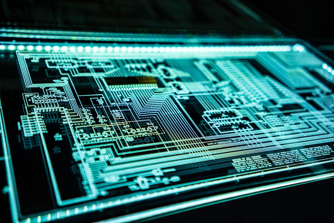
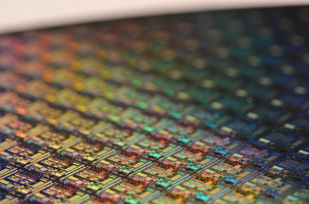
The researchers used the tools of conventional chip technology to develop the artificial graphene in a standard semiconductor material, GaAs. They designed a layered structure so that the electrons could move only within a very narrow layer, effectively creating a 2D sheet. They used nanolithography and etching to pattern the GaAs: the patterning created a hexagonal lattice of sites in which the electrons were confined in the lateral direction. By placing these sites, which could be thought of as 'artificial atoms' sufficiently close to one another (~ 50 nanometers apart), these artificial atoms could interact quantum mechanically, similar to the way atoms share their electrons in solids.
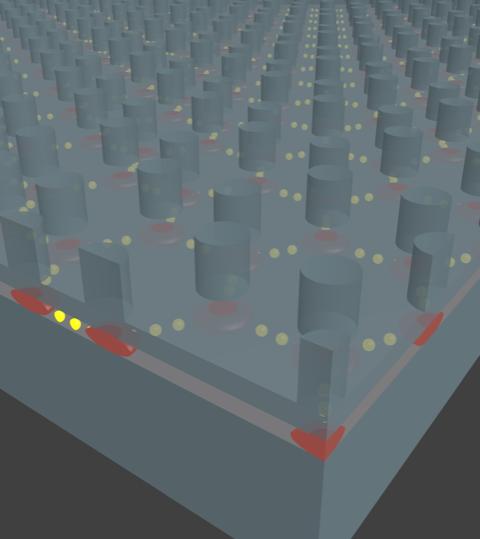
In the picture above, etched pillars define the positions of quantum dots (red puddles) arranged in an hexagonal lattice. When the spacing between the quantum dots is sufficiently small, electrons can move between them.
The team probed the electronic states of the artificial lattices by shining laser light on them and measuring the light that was scattered. The scattered light showed a loss of energy that corresponded to transitions in the electron energy from one state to another. When they mapped these transitions, the team found that they were approaching zero in a linear fashion around what is called the 'Dirac point' where the electron density vanishes, a hallmark of graphene.
This artificial graphene has several advantages over natural graphene: for instance, researchers can design variations into the honeycomb lattice to modulate electronic behaviour. And because the spacing between the quantum dots is much larger than the inter-atomic spacing in natural graphene, researchers can observe even more exotic quantum phenomena with the application of a magnetic field.
The discovery of new low-dimensional materials, such as graphene and other ultrathin, layered van der Waals films that exhibit exciting new physical phenomena that were previously inaccessible, laid the groundwork for this study. "What was really critical to our work was the impressive advancements in nanofabrication," Pinczuk notes. "These offer us an ever-increasing toolbox for creating a myriad of high-quality patterns at nanoscale dimensions. This is an exciting time to be a physicist working in our field."
"This is a rapidly expanding area of research, and we are uncovering new phenomena that couldn't be accessed before," says Shalom Wind, faculty member of the department of applied physics and applied mathematics and co-author of the study. "As we explore novel device concepts based on electrical control of artificial graphene, we can unlock the potential to expand frontiers in advanced optoelectronics and data processing."
"This work is really a major advance in artificial graphene. Since the first theoretical prediction that system with graphene-like electronic properties may be artificially created and tuned with patterned 2D electron gas, no one had succeeded, until the Columbia work, in directly observing these characteristics in engineered semiconductor nanostructures," says Steven G. Louie, of physics, University of California, Berkeley. "Previous work with molecules, atoms and photonic structures represent far less versatile and stable systems. The nanofabricated semiconductor structures open up tremendous opportunities for exploring exciting new science and practical applications."
'Observation of Dirac Bands in Artificial Graphene in Small Period Nano-patterned GaAs Quantum Wells' by Sheng Wang et al; Nature Nanotechnology (27th November 2017)