PIC manufacturing: solutions for optical communicationsÂ

Nick Psaila, CEO and co-founder of Optoscribe, shares his perspective on the prospects for PICs and gives his view on what's required to capitalize on growth in silicon photonics and other key platforms.
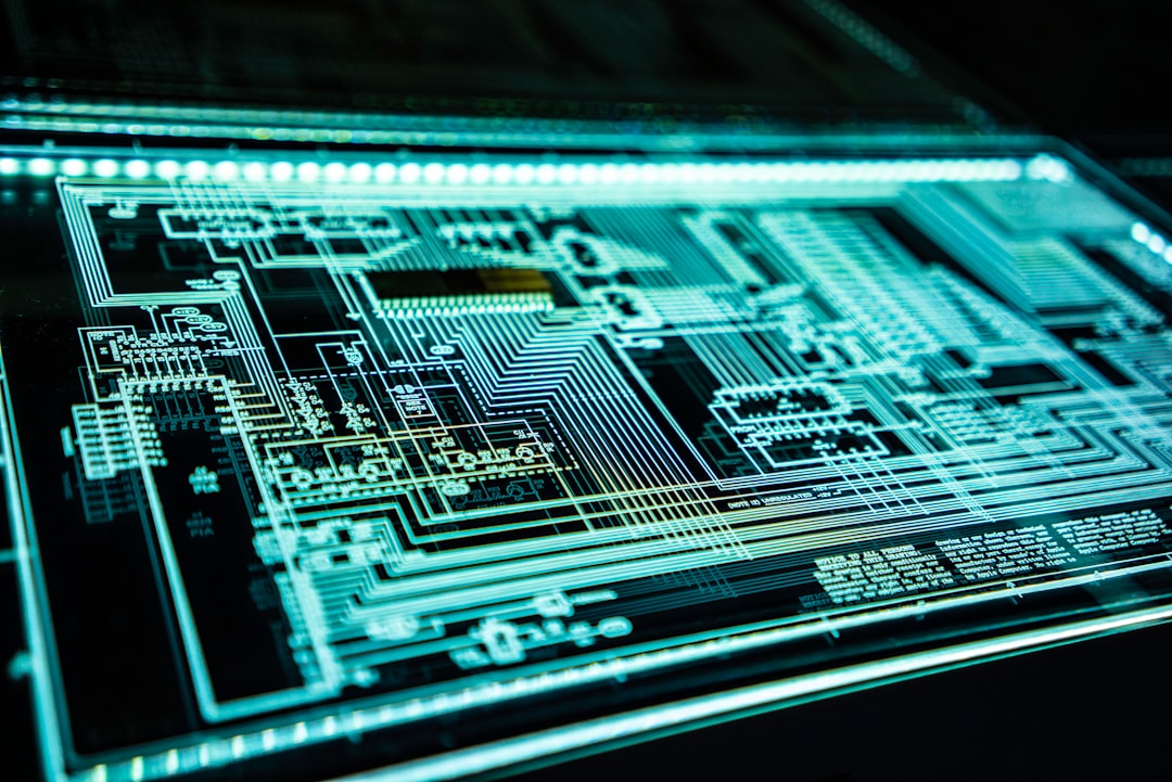
Within photonic integrated circuit (PIC) manufacturing, there are some impressive developments happening both at subcomponent level and in device integration. PICs are progressively becoming more complex, and are commonly including a lot of aspects which in conventional waveguide platforms would have been challenging to implement only a few years ago. However, there is still the fundamental challenge of assembling this chip into a package, connecting it up both optically and electrically, and achieving all of this in a low loss and robust way.
This is particularly the case when it comes to the optical connections inside the package. For example, potential height offsets between one end and the other can be problematic, and the alignment tolerances required for many different PIC technologies is particularly tight causing significant challenges. There are several ways people are trying to address this in the industry and various structures are made both on and outside the PIC to try and alleviate this problem.

Optoscribe's new facility in Livingston, Scotland. The 7,400 square foot building, which opened in March 2017, includes a mixture of Class 1,000 and Class 10,000 cleanrooms.
Fundamentally, for most PIC technologies you ultimately have to use some form of active alignment during assembly. This may result in the best insertion loss but it is certainly a limiting factor in terms of throughput and cost of assembly. This is particularly a concern for high volume data centre applications, where data centre operators are very keen for transceiver manufacturers to move to an electronics assembly type of model, which will help drive the cost per gigabit down to the data centre operators' target of <$1 per gigabit/s for single mode optical transceivers. However, this target will not be achieved using complex and costly assembly processes. The photonics industry must focus on what can be done to adopt electronics style assembly processes. In addition, some PIC designs require hermetic packaging, which adds significant expense. Alternative technologies that avoid fully hermetic sealing should be deployed wherever possible to eliminate this costly element.
Volume is key
I am very optimistic for the expansion of PIC technologies. I think platforms may achieve a higher market share than perhaps many market reports forecast. The technology has the capability to displace current incumbent, alternative technologies and with enough investment PICs could drive overall product cost down, and meet data centre operators' challenging cost aspirations.
With enough volume, silicon photonics can become very cost effective due to the well-established silicon foundry model inherited from the electronics industry, providing it can be packaged cost effectively. To succeed, volume is the key. Once the critical volumes are achieved we will quickly see the cost and yields reach the target levels "“ historically MEMS followed this same path.
At the moment, vertical cavity surface emitting lasers (VCSELs) are dominant because they are very low-cost and reliable, but most large data centre operators have a roadmap to single-mode-only architectures which we know is a challenge for VCSELs. If Indium Phosphide can scale in the wafer size and chip complexity, whilst maintaining good yields, there is a chance it could make a dent in data centre client-side interconnects. However, to date the cost has mostly limited this to telecoms and line-side data centre interconnect (DCI) applications. As it stands however, I believe silicon photonics has a key opportunity to dominate at 400G and beyond within the data centre. There are many in both camps that are fighting to gain market share.

Scalable solution: 3D optical waveguides created using laser inscription.
Fundamentally there has been so much investment and rapid technology development in silicon photonics, that it is very difficult to see it not having a very big part to play in the future of optical interconnects.
The ability to increase the density of optical channels in a package is a significant benefit. On the PIC side it reduces the chip surface area used for the optical interface, which can help to reduce cost. As the size of the PIC becomes smaller, the need for compact fibre coupling solutions such as Optoscribe's monolithic glass 3D fibre coupling platform becomes a necessity. This compact and precise type of coupling platform brings significant benefits and with the move to larger optical channel counts and potentially multicore fibre, which has an inherent density advantage, this smaller footprint will become even more important.
Optoscribe brings other benefits to enable electronics style high volume manufacturing processes for optical transceivers. Products made using these kinds of processes typically use pick and place for ball grid array components and these often need to go through a solder reflow process, which is problematic for many conventional packaging materials such as epoxies due to the high temperature profiles.
An expanding market
I think both Optoscribe and PIC technology have applications in wider telecoms networks as well as datacoms. Starting with the shorter-range side of the network, including potentially 5G mobile infrastructure, there will be a gradual move into longer range market segments as time goes on. On the long haul and ultra-long haul side of the telecoms network there are a number of well-established incumbents using discrete components, which could be hard to displace in the foreseeable future. However, in other segments such as data centre interconnects there is already a precedent of PICs being deployed.
In addition to this, PICs have a bright future in general purpose computing interconnects. As transceiver functionality transitions from pluggable modules to on-board to co-packaged and ultimately embedded alongside processing electronics, PIC technology will be able to play an increasingly important role in providing high-speed low-latency links as the interconnect requirements for high-speed electronics scales further.
From there, PIC technology will eventually find its way into everyday computing, and eventually right into consumer electronics. As key industry luminaries have talked about for some time, electrical interconnects have become a particularly significant source of power usage in modern high-speed computers and information processing electronics. Integrated photonics has the opportunity to significantly reduce the power consumption involved in data transmission, including within the next generation of electronic integrated circuits.
Business growth and development
One of the biggest challenges has been building an understanding of the market intelligence to give Optoscribe the independence to be able to take the technology to market. Also, it's very important to build the right team around the technology, with employees who can transition as the company matures. As the firm evolves from its very early stage, with just a few people, and starts to scale and grow you require a different type of person.
It is important to realise that this transition needs a specific skill set and that you need to bring in people who have the appropriate experience. This covers all aspects of the business from sales and marketing through to operations and technical management. As the teams grow, the skill sets for managing teams becomes critically important to bringing the company success. Equally important is having the right investors, and finding investors that are willing to support a particular type of business; in our case, innovative hardware technology. We had to find investors that are keen to support a high-tech manufacturing business that involves some level of capital investment in a manufacturing facility and capital expenditure.
Finding the correct type of premises and location for the business to operate in with access to the relevant staff in the area was important. Fortunately, the optical sector has a good presence in Scotland, which means there is access to a highly educated, skilled workforce, and this has been very beneficial in building the company.
Lessons in starting up
In terms of taking technology from a university environment to a high technology manufacturing model, there was the typical naivety at the early stage where companies have aspirations to address everything under the sun. Then the quick realisation that it is absolutely not a feasible way to build a business and you quickly learn to whittle down to areas in which the technology has the potential to disrupt a growing market.
One important advantage with the type of technology we offer is to be able to provide a customisation service and offer customers a quick turnaround of prototypes configured precisely around their product design. To carry out the range of activities here using conventional lithographic technologies would require a substantially larger workforce and facility. The technology and the automated processes we have developed allows us to do a great deal with the current team of 25 employees.