EV Group reports increased demand from wafer-level optics
Demand for manufacturing solutions driven by consumer electronics, mobile and other applications requiring advanced 3D / optical sensors
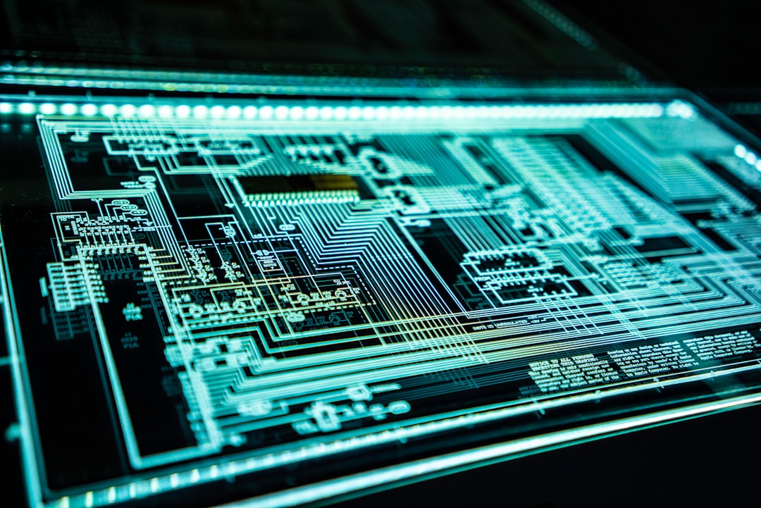
EV Group (EVG), an Austrian supplier of wafer bonding and lithography equipment, has announced that it has received multiple orders for manufacturing equipment and services designed to address the burgeoning demand for wafer-level optics (WLO) and 3D sensing.
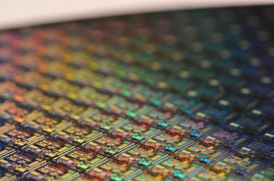
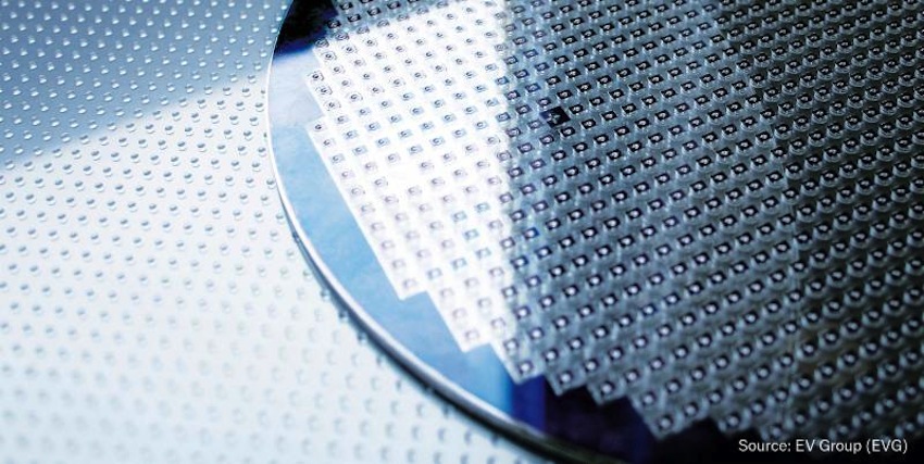
Equipment includes the EVG770 automated UV-nanoimprint lithography (UV-NIL) stepper for step-and-repeat master stamp fabrication; the IQ Aligner UV imprinting system for wafer-level lens molding and stacking; and the EVG40 NT automated measurement system for alignment verification. (Shown above is a lens wafer fabricated with the IQ Aligner soft UV imprint lithography technology, and a bonded micro optics stack consisting of lens wafers and spacer wafers.)
"We are seeing a steep increase in the demand for equipment enabling wafer-level optics," confirmed Thomas Glinsner, corporate technology director for EV Group. "Since the beginning of this year alone, we have shipped multiple systems for lens molding and stacking as well as metrology to major WLO manufacturers for high-volume production. Such orders are further strengthening EVG's position as the market leader in this area, while creating a wealth of new opportunities in emerging applications."
Demand for EVG's WLO manufacturing solutions is driven in part by the need for novel optical sensing solutions and devices for mobile consumer electronics products. Key examples include 3D sensing (essential for more authentic virtual and augmented reality (VR/AR) user experiences), biometric sensing (increasingly critical for security applications), environmental sensing, infrared (IR) sensing and camera arrays.
Other applications include additional optical sensors in smartphones for advanced depth sensing to improve camera autofocus performance, and micro displays.
"There is undoubtedly a highly sustainable trend emerging in wafer-level optics and 3D sensing," stated Markus Wimplinger, EV Group's corporate technology development and IP director. "We foresee even broader adoption of this technology in the near future due to the large number of ongoing customer projects supported by our NILPhotonics Competence Centre located at our corporate headquarters."