Q&A: fulfilling a vision for high-speed interconnects

In 2017, Sicoya -- a Germany-based developer of highly-integrated silicon photonics and spin-out of TU Berlin -- launched its first products into the data centre market. Sven Otte, the firm's CEO, explains why we need Photonic Integrated Circuits (PICs) to deliver high-speed transceivers in the large quantities that customers are calling for. Interview by James Tyrrell.
Q1 - What do you see as the big benefits of PICs and how is Sicoya applying this technology to deliver attractive solutions to its customers?
We are now going into an era in which we need ultra-high speed transceivers. Huge demand is being driven by both machine-to-machine communication and mobile communication, but applying discrete manufacturing approaches to 100x higher volumes is impractical - the cost doesn't scale with volume any further and quality can be affected. Photonic integrated circuit (PIC) technology addresses these challenges - the volume constraints quality and cost.
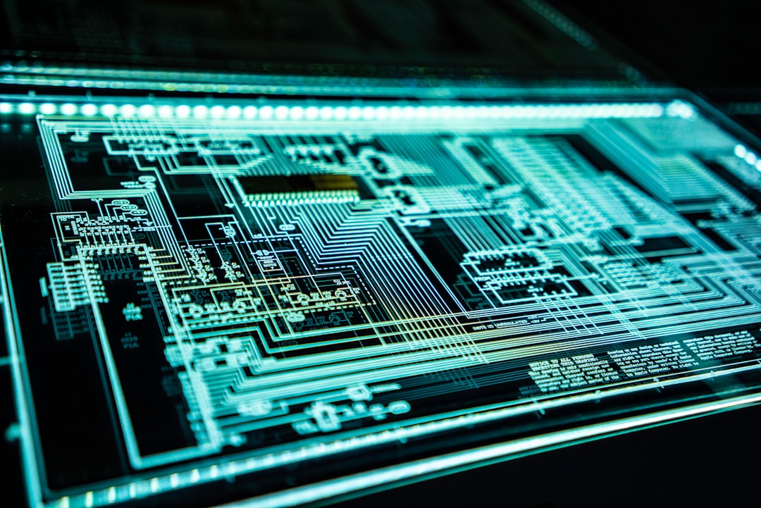
Co-integration solution: Sicoya's transceiver chips feature analog electronics and optics fabricated, using SiGe-BiCMOS process technology.
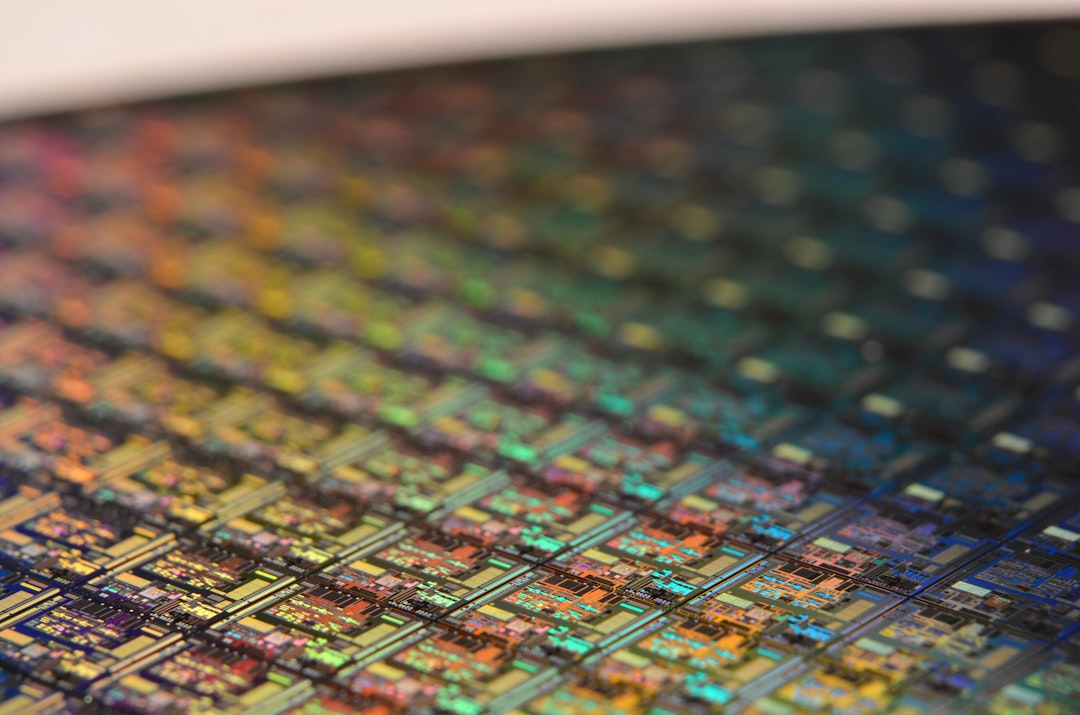
There is some debate in the industry about which PIC technology to use "“ for example, are silicon (Si) or indium phosphide (InP) PICs better suited for future solutions? But we see different PIC platforms becoming commercially available and that's good because each technology addresses a specific problem. Silicon is the better material system from a manufacturing point of view. It is, practically speaking, available in abundance and offers outstanding material properties when, for example, looking at the number of crystal dislocations or the surface quality. As a result, the cost of Si is 10x lower than InP. In addition epitaxial growth and lithography processes in Si outperform their InP counterparts. From here we can easily see why processing 300mm Si wafers with very high yields is achievable while the size of InP wafers is limited to 80mm and yields are lower.
Silicon devices, both the electrical and the photonic components, tend to be much smaller because of the lithography processes and the material properties - for example, we can build very high-speed modulators that are less than 100 micrometers long in Si while in InP the same modulator is around a centimetre in length. Overall, this leads to a situation where all building blocks that can be achieved in Si will be made using Si eventually. Obviously, Si is an indirect semiconductor and hence cannot generate photons. So, consequently, we will continue to use InP, but only where needed - for example, to create the laser.
However, even lasers can be broken down into subparts such as the gain medium and the grating. Gratings can be made in silicon and for the gain medium a thickness of a few hundred nanometres is sufficient, which can be integrated in a CMOS process. Indium phosphide may therefore become a complementary material in an overall Si wafer manufacturing flow just like germanium is in today's BiCMOS processes, for example. This however is in the future. Today InP and silicon photonics co-exist.
At Sicoya, we bring the integration approach to the boil and we are combining entire transceivers into a single Si chip, which we call "˜Module-in-Chip' (MiC) technology. All electrical transceiver functions such as clock and data recovery, control loops, amplifiers, modulator drivers and all optical functions including modulators, multiplexers and photodetectors are integrated in one small chip. 
From the lab to the market: Sicoya aims to bring integration "˜to the boil', delivering feature-rich devices in a small package.
We benefit from the manufacturing technology of our commercial BiCMOS foundry and achieve the same quality and cost data compared with conventional BiCMOS processes "“ that is a promise that has been made in the past already and is now a reality. Additionally, we have developed a 3D packaging concept which allows us to put our MiC engines very much like standard semiconductor packages.
Another element of our know-how are the devices itself. In semiconductors one can differentiate by the way transistors and resistors are put together inside the chip - that is, by the circuit design. Photonic circuits are in comparison much simpler and differentiation is only possible on device level. At Sicoya it took us more than 10 years to develop and patent the devices that we are now using in our products.
Q2 - Can you talk about the journey from idea to device - what do you see as the challenges in making the most out of PIC-based platforms?
Our journey began 2006 when we started to develop the basic process and device technology. This was research at its best and we are grateful for all the support which was coming from national and EU resources. Now we are entering the commercial stage, and development cycles for new products need to come down from 10 years to 1-2 years. This represents a challenge from various aspects.
To highlight one area, PIC platforms generally tend to have a research background with outstanding technology capabilities, but at the same time it's important to also have the internal processes to support agreements on delivery, price and quality details. Assume, one develops a product on a PIC platform, which cannot support a commercial business. It would mean that the design must be transferred to another foundry, which typically isn't possible over a short time frame. We are in a fortunate position to have an EPIC (Electronic-Photonic-Integrated Circuit) platform which supports both research and high-volume commercial business and I expect that more platforms follow this example in future. It's worth adding that this example is not limited to PIC foundry platforms - it applies to packaging services as well.
Q3 - 2017 is sounding like a very exciting year for the company with the launch of your first chips for use in data centres. Looking ahead, what's your vision for future internet services? Where could PIC technology take us?
Yes, indeed "“ 2017 is a super exciting year for Sicoya and we are getting great feedback across the globe. Our initial 100Gb/s products are just the beginning as we keep pushing the possibilities and features of the EPIC technology. It's an amazing start and you can expect much more to come in the next 1-2 years.
If we look at industry trends, data rates are moving from 100Gb/s to 400Gb/s and we can achieve this at lower cost and with better performance. We are also actively driving a change in the way standards are written. When you have all optical and all electrical signals available in one chip, this opens up the possibility for new types of products. As photonic AISICs become available in a semiconductor package why not eliminate a few switch hierarchies in a data centre? I am not talking about a one-by-one replacement of copper with optics. Rather, it's a change in the architecture of data centre in which servers and storage devices are connected to the network optically without copper and switches in between.
We also see interesting things happening in the IoT and sensor area where PICs can be an enabling technology for new products. The future for (E)PICs is bright and we are glad to be part of it.