Photonic integration: the key to unlocking future innovations in optics
The growth in cloud-based services and other bandwidth-intensive applications sets the scene for further advances in PIC technology. Adam Carter, chief commercial officer at Oclaro, looks at some of the developments coming through into the market and the various processing steps required to create a device.
The global communications market's insatiable demand for higher bandwidth, higher density, lower power consumption and continued cost reductions has been driving the optical industry for years. However, we have now reached bandwidths where photonic integrated circuits (PICs) "“ particularly on indium phosphide (InP) "“ are critical if we want to keep this innovation moving forward. Network providers and data centre operators are struggling to keep pace with the demand for cloud-based services and other bandwidth-intensive applications. In order to provide the bandwidth they need, optical companies are tasked with increasing the aggregate bandwidth at the front panel, improving the performance, and reducing the power consumption "“ all while also lowering the cost. As optical devices become more integrated and more complex, achieving these bandwidth requirements is becoming increasingly difficult. This is where photonic integration comes into play "“ and will for many years to come.
Increasing front-panel bandwidth
To deliver the bandwidth the industry requires, optics companies need to increase the data rate of the individual modules. This will increase bandwidth per slot at the system faceplate (i.e. 10 to 40 to 100 Gbs) not only for short reach intra-data centre connections (<10 km), but also for inter-data centre connections >100 km. Currently, for inter-data centre connections, bandwidth requirements are already transitioning from 100 Gb's (DQPSK modulation) to 200 Gbs (16 QAM modulation) and higher. The transmission technology used for inter-data centre connections is becoming much more "analog like" in terms of increasing constellation density and bandwidth. While there is less dramatic change in the core III-V technology as bit rates increase, it is becoming more important to focus on improving cost, power and faceplate density. This is where photonic integration plays a crucial role.
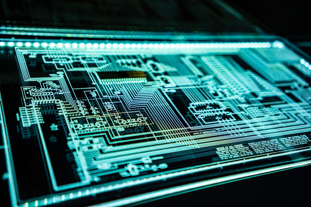
A perfect example of this is the CFP2-ACO, a pluggable analog coherent optical module shipping in volume today from technology leaders such as Oclaro. Photonic integration has been key to delivering the high performance, low power dissipation and small size of the current generation of CFP2-ACO modules, with the transmitter PIC having Mach Zehnder modulators (MZM), semiconductor optical amplifiers (SOA), integrated optical power monitors, as well as different test structures incorporated onto a single chip.
With the CFP2-ACO, customers are provided with one module that integrates all the optical functionality needed for 100 G or 200 G DWDM transmission with the added benefit of pluggability for reduced first installed cost. With this CFP2 footprint, customers can integrate up to 8 CFP2s on a 1 RU line card, enabling a faceplate bandwidth of 1.6 Tb at 200 Gbs per slot.

Figure 1. Photonic integration: Oclaro's CFP2-ACO pluggable transceiver features a transmitter PIC with Mach Zehnder modulators (MZM), semiconductor optical amplifiers (SOA), integrated optical power monitors, as well as different test structures incorporated onto a single chip.
In addition to the CFP2-ACO, Oclaro also has a long history of delivering photonic integration for its 10 G tunable product family. Although less complex than the chips used for the ACO transceiver, this family has been the proving ground for the design, modeling and process technology needed to integrate a variety of structures in InP such as a tunable laser and a Mach Zehnder modulator. These tunable modules have built up an extensive number of deployed hours across global networks, a development which has helped to substantiate the reliability of photonic integrated devices.
The benefits of integration in the intra-data centre market are a little further in the future as the industry can currently accommodate up to 32 QSFP+ ports enabling 3.2 Tb of aggregate bandwidth on an 1RU faceplate. Today, this can be done using discrete externally modulated lasers (EML) or directly modulated lasers (DML) depending on the specific application required. However, as bandwidths per slot increase, the industry will need to incorporate different higher order functionality and modulation schemes such as PAM4 to enable continued scaling. This will put added design restrictions on optical component companies as they strive for reductions in module size and power consumption to enable high density in higher bandwidth applications. History has proven that higher-order functionality will eventually transition out of the optics modules and into the physical layer SerDes ICs on the linecard. This will then enable simpler, smaller, and more cost-effective optical modules, which will benefit from higher levels of photonic integration at the chip level.
Challenges at the device level
There are many challenges to integrating all the different functionality required on today's PICs. However, once a company has a platform photonic integration process that is not geared to only one specific function, this integration becomes much simpler. This does not, however, happen overnight. It takes many years of experience and development investment to establish the methodologies, processes and designs to produce reliable PICs that can be packaged, tested and shipped for specific customer applications. As an example, Oclaro has spent many years transitioning from discrete III-V devices to photonic integrated circuits. To enable these higher levels of integration, the company has primarily focused on developing wafer fabrication processes to drive high yields in manufacturing for these complex chips. Many thousands of man hours have been spent developing an integration process that enables Oclaro to mix and match a variety of features/components on a single chip. These are all effectively connected together, aligned photo lithographically at the nanoscale, and fabricated with common process steps in multi-wafer batches. During the initial design stage of a new PIC, we strive to minimise the chip area similar to what is done in the silicon industry. This reduces cost as you increase the number of chips/wafer. Process control in the wafer fab is paramount and we constrain our designs to ensure manufacturability and high yields. In essence, we "design for the fab" and not "fab the design."
Another challenge is that generic packaging is not always possible for PICs as the variety of functions needed are very diverse and require specific RF, DC, thermal and optical interfacing that are specific to the application. This can add extra levels of complexity and increases the level of resources required during product development. In fact, the packaging development can be more complex than the actual chip itself. Thus, access to the PIC is only one part of the product development cycle.
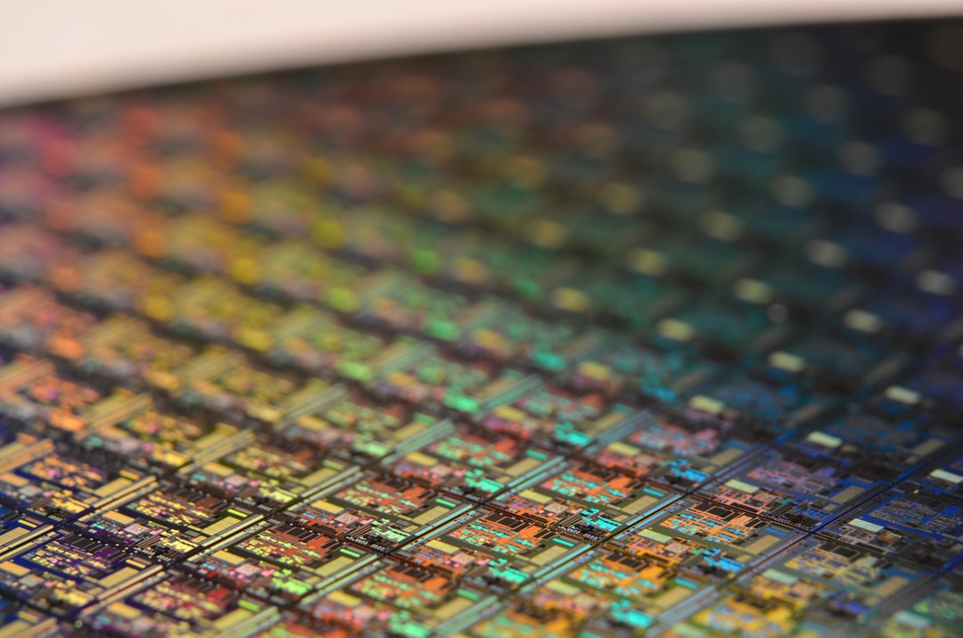
An example of PIC process flow
The following image depicts the various processing steps involved in producing a PIC for an integrated laser modulator.

Figure 2. Building a device: schematic view of the various steps required to produce a photonic integrated circuit for an integrated laser modulator.
What is not captured in this schematic is the design, modelling and layout work that is needed before the processing of the PIC actually starts. More work in the industry is needed to further develop the tools, library elements and layout automation, but with the many years of experience developed at Oclaro, we can turn new designs quickly and have sufficient tools to ensure correct functionality and performance is obtained on the initial design.
A critical additional step is to do as much testing as possible at the wafer level rather than on the individual PIC itself. By automatically identifying known good die for assembly, yields can be kept high through the later stages of packaging and module manufacture. It also enables optics companies to map all key parameters at the wafer level to maintain process control and integrity throughout the III-V manufacturing line.
Bringing high-performance, high-value solutions to customers
The evolution of the hyperscale data centre and cloud provider market has led to a more rapid transition between data rates due to the ever-increasing need to support more bandwidth intensive applications. For companies such as Oclaro, this means that our conventional product development timescales are continually being challenged to become shorter without compromising on cost or performance. One of the ways we combat this is to develop the PICs well ahead of when the modules require them or even before a standard has been generated. This ensures that the chip development cycle time does not impact the product development time. For example, today Oclaro is already developing the next generation WDM PICs for higher-bandwidth coherent applications.
Our customers in the markets we serve are particularly interested in higher bandwidths (400-600 Gbits) achieved using higher electrical baud rates in combination with higher capacity modulation formats (64 QAM.) These have to be achieved while continuing the innovation needed to increase faceplate density, reduce power consumption and drive a lower cost structure. With photonic integrated devices already shipping in volume in the form of tunable lasers and the CFP2-ACO, the industry can expect continued use of photonic integration, particularly in the metro, data centre interconnect and long haul markets. Photonic integration will enable our customers to solve some of their largest problems around increasing operational efficiencies and scalability.
Future advances in photonic integration
The increasing importance of time to market (TTM) for high bandwidth solutions for both telecom and datacom applications will demand better design automation and packaging solutions for PICs. The same fabrication equipment that is used in conventional discrete laser fabs today can still be used. However, as the complexity and functionality of PIC designs increases, we will need even greater process control and design methodologies to achieve the capacity levels and cost points the industry needs, particularly as demand for cloud based services increases.
Testing and qualification are also things to be considered in the future because in the coherent world, as an example, we are seeing a clear dependency between the electronics and optics and how they contribute to the end system's performance. For qualification, today's standards were written more for discrete components. As integration advances, these procedures and methods become less appropriate for photonic integration. If we look at an example where only a few elements in the circuit design in a new product are different from the existing design, all the data from previous qualifications on the laser can be read forward into the new product, reducing the time to complete qualification and reducing development costs. Furthermore, we are already seeing major changes in likely deployment lifetimes between traditional Telecordia requirements and the data centre markets where five-to-seven year deployment lifecyles are typical.
To enable future advances in photonic integration, it is also essential that the wider ecosystem is expanded. Oclaro is aggressively working with equipment suppliers, users and academia to promote, sponsor and supervise research on areas including PIC technology (not just InP), layout methods, modeling, manufacturing, applications and systems.
Summary
Photonic Integration is a key technology for enabling optical component companies to meet the ever-demanding requirements of its customers to efficiently scale their networks while also driving productivity gains. The use of complex photonic integrated circuits will enable them to meet this demand by enabling higher faceplate density and lower power consumption. This will be critical for meeting the continued bandwidth demands of the future.