Q&A: exploring the use of integrated optical platforms in IT and beyond
James Tyrrell interviews Bert Offrein, manager of the photonics group at the IBM Research Laboratory in Zurich, to find out what makes PICs so appealing and to discuss opportunities where developers can team-up to smooth the path for wider adoption of novel devices.
What do you regard as the major benefits of photonic integrated circuits and where do you see the technology making an impact in the field of information technology?
The major advantage of photonic integrated circuits lies in the ability to combine several functions in one wafer scale platform. This enables a cost-effective integration of multiple structures through parallel processing means. Photonic integrated structures help to reduce the assembly effort associated with combining discrete devices and provide higher density smaller form factor solutions. In optics, the excellent stability of integrated structures is another important aspect - for example, in phase sensitive applications.
What stage are PIC devices at today and what are the prospects further out from a chip perspective?
Several integrated optical platforms exist such as glass on silicon, III-V and silicon photonics. Today, all these platforms are important for commercial applications and multi-project wafer based foundry offerings are available. Integrated optic devices are found in a wide range of applications for tele- and data-communications, sensing and others. The current trend is towards combining various platforms such as silicon and III-V technology to further enhance functionality, density and efficiency of the devices.
Tell us about your group and the areas you are focusing on - what are the current challenges and highlights of your research so far?
In my group at IBM Research - Zurich we have developed various integrated optical technologies such as a silicon-oxynitride glass on silicon technology for high density dynamic passive optical devices, polymer waveguide based optical printed circuit board technology and silicon photonics. We have brought all these technologies to a high-level of maturity in collaboration with partners. With our IBM colleagues in North America, we demonstrated a 100 Gb/s WDM link in CMOS silicon photonics. Our current focus is on electro-optical assembly of silicon photonics devices where we demonstrated ultra-low loss polarisation independent fibre-chip coupling that is broadband and scalable to many optical in- and outputs. Another focus is the integration of III-V materials onto silicon photonics to embed optical sources into the silicon photonics chip, together with passive optical functions and CMOS circuitry. The chip-level combination of all these functions has the potential to drive many new applications.
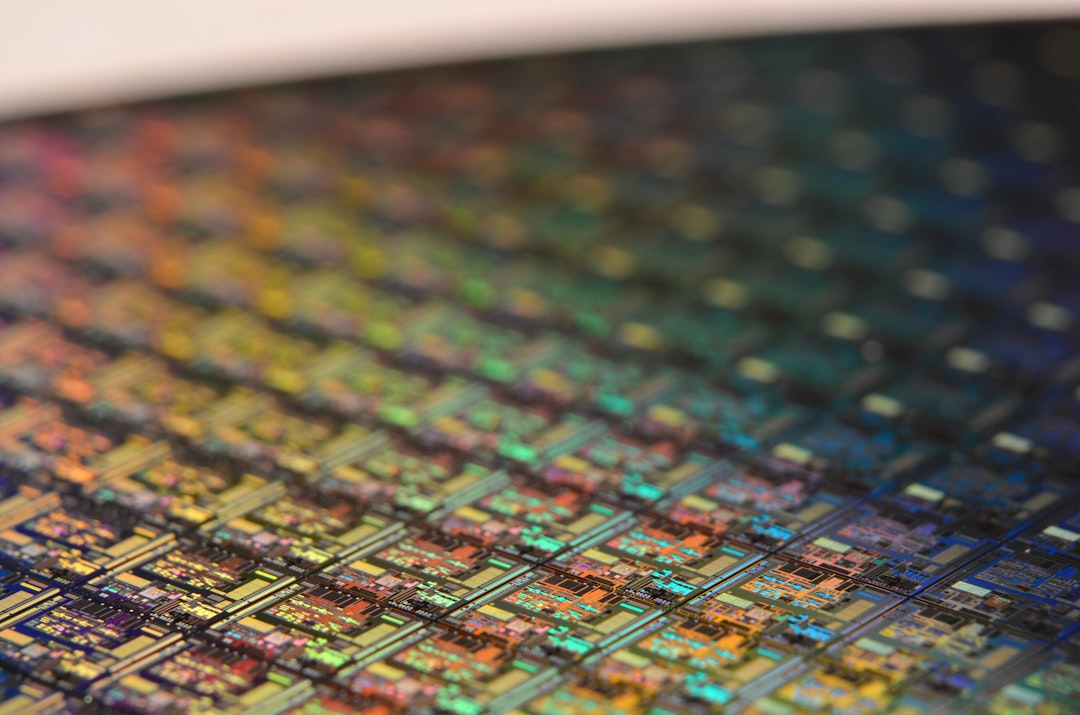
Figure 1. IBM silicon photonics: a cassette carrying several hundred chips intended for 100 Gb/s transceivers. The dense monolithic integration of optical and electrical circuits and the scalable manufacturing process provide a cost-effective silicon photonics interconnect solution, suitable for deployment in cloud servers, data centres, and supercomputers. Credit: IBM
Photonic integration presents a tremendous number of opportunities across a wide range of fields. To make the most of its potential, what do you see as the priority areas where the community needs to team up - for example, to solve challenges in packaging, standardisation, road-mapping or supply chain development?
Today, we see a range of photonic platforms being developed. Although this is diluting resources, ultimately this range of activities is required to sort out the optimum solution for the applications available. Also in electrical CMOS technology we see a wide variation of "˜flavours' to meet all application requirements. Teaming up is definitely required in standardisation, defining common interfaces to the outside world, but also inside the system. In addition, roadmapping and defining future needs is something that people should team up for.
Figure 2. Optical connectivity: polymer waveguides offer an integrated approach to realising high-density connections over short distances, replacing multiple electrical cables. Credit: IBM


