Customised packaging for PICs
Augmenting traditional transfer moulding with Film Assisted Moulding and Dynamic Insert Technology can deliver a range of benefits to PIC makers. As well as providing necessary packaging attributes, the approaches allow additional functionality to be inserted such as lens structures or through polymer vias. Marco Koelink of the Advanced Packaging Center in The Netherlands provides an overview of the technology, including recent developments in die-attach, and shares device examples from solar, automotive and other key sectors.
Photonic Integrated Circuits (PICs) are developing very rapidly to become one of the most promising technologies for fabrication of functionally advanced, compact and cost-effective optoelectronic devices. Enabling this cost and performance breakthrough is the ability to produce PICs using existing and standard semiconductor processes (Piramidowicz at al [1]). However, in order to benefit fully from these advantages both the front-end (monolithic integration) and the back-end (packaging) needs to deliver device solutions that meet cost and performance targets.
Transfer moulding has been the primary process method for microelectronic encapsulation using epoxy moulding compound (EMC). The technology can scale to meet high-volume demands and low-cost requirements. However, traditional transfer moulding has disadvantages such as EMC bleed and resin flash, time consuming mould cleaning, mould wear, package deformation during the ejection process and lead frame deformation or (ceramic) substrate cracking due to clamping.
Dealing with the challenges
Film Assisted Moulding (FAM) offered by the Advanced Packaging Center (APC) deals with these challenges - releasing the compound from the mould and keeping certain surfaces ("windows") clean from moulding compound. These windows can facilitate emitting or sensing areas of an optical chip. In addition, Dynamic Insert Technology (DIT) has been developed to further optimise the performance of FAM to automatically and dynamically control pressure on one or multiple surfaces while adjusting for height differences and tilt (compensating for most of the tolerances).

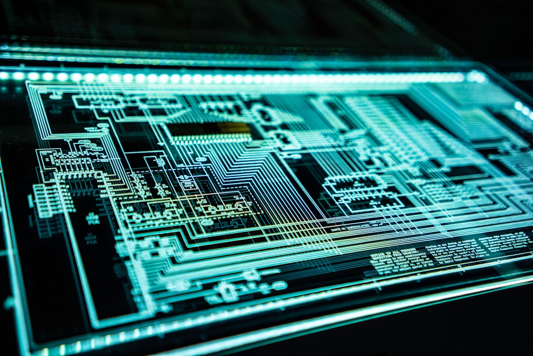
Figure 1. Schematic overview of the application of Film Assisted Moulding (FAM) Technology and Dynamic Insert Technology in transfer moulding.
The diagram above shows a schematic representation of the application of FAM and DIT in transfer moulding. A more detailed description of FAM and DIT can be found in Bos et al [2]. These technologies enable the use of many different compound materials (epoxy, silicone) that can be applied in different versions (black, white, clear and combinations thereof). The base materials can also be solid or fluid. In combination with the use of different die-carrier materials such as lead-frames and different substrates (ceramic, metal, FR4, wafer-level) and the option to design exposed open windows in the package, a large variety of packages can be designed to meet the needs of different applications, including optical applications.
Packaging requirements
Recent developments in PICs, solid-state lighting, communication technology, (medical) sensor technology and other areas require optical packaging solutions that meet both the electrical and optical requirements and allow for high-volume production at reasonable costs. Optical requirements may include total encapsulation (environmental ruggedness), but with defined optical transparency. In other cases, the optical components should be fully exposed to the environment (exposed window). Also, some optical interfacing to the environment might be desirable (connections to optical plastic fibres, lenses for enhanced field of view). Electrical requirements may include a number of IOs, (high) voltage ruggedness, and mechanical requirements may include a defined package layout (for example - QFN, SO, DFN, BGA, LGA or customised), a defined operational temperature range and mechanical ruggedness. Furthermore, designs need to meet different standards, such as automotive or industrial. All of these combinations are well within range of the technology presented.
Compound materials selection
Transfer moulding using FAM/DIT allows for many different compound materials and even combinations of different materials. Epoxy based materials and silicones are most widely used and come in black, white and transparent versions. Traditionally, for microelectronic encapsulation a black compound is used. This consists of an epoxy resin filled with a possible variety of materials (graphite, metal oxides, glass, silicon oxides, etc) that create the colour and a matching coefficient of thermal expansion (CTE) to semiconductor materials. The colour black is preferred because various electronic components are sensitive to light. Similarly, a white compound can be used. In this case, the material consists of a similar epoxy resin containing fillers such as TiO2. These materials can be used to enhance reflectivity of a package or influence the direction of emission patterns of optical sources. An epoxy resin without fillers can be used as a transparent compound. These materials can be used to encapsulate optical components while maintaining optical transparency. However, epoxy resins usually have a large CTE mismatch compared with semiconductor materials, which requires sufficient attention in the design phase to avoid thermo-mechanical stress.

Figure 2. An LED system design using a black epoxy to encapsulate an ASIC (green). Wire bonds and a transparent silicone compound with incorporated lens shape are also shown.
An alternative to epoxy resin is silicone, which has some interesting properties. It is a much softer material than epoxy resin, leading to much less thermo-mechanical stress. It is much less susceptible to optical (UV) degradation, making it ideal for applications with long life-time requirements and high radiation levels (for example - concentrated photovoltaics, as shown below). However, because the material is soft, it can be hard to saw, which can be difficult for high-volume production. Silicone compound is a fluid based material which makes it difficult to use and absolutely requires double-film based moulding (FAM).

Figure 3. Examples of a solar collector (concentrated photovoltaic) in a white compound.
Substrate selection and package layouts
Transfer moulding is a flexible technology, which allows for many different substrates to be used. The traditional lead-frame technology has many advantages - it is a well-known technology, has good adhesion properties to compound materials, it is cost-effective in mass production and allows many different technologies for die-attach (gluing, soldering, welding, sintering etc). Alternatively, different substrate materials can be used: metal, ceramic, flex-foils, FR4 or wafer-level. FR4 materials (or similar) can be tricky: at elevated temperatures they can outgas leading to decreasing adhesion. The use of double-film based moulding (FAM) enables large areas of substrates to be free of compound, which can be advantageous for secondary level packaging or thermal considerations.

Figure 4. Left: a lead-frame based design for an automotive optical transceiver. The devices are fully encapsulated in clear compound with integrated alignment bumps to facilitate the in-coupling of light into a plastic optical fibre. Middle: a lead-frame based design for a photometric sensor, fully encapsulated in clear compound. Right: a fully integrated (analog and digital) optical sensor system in a similar lead-frame bases design fully encapsulated in clear compound with a small optical lens in the right bottom corner (see also figure 6, left) .
Wafer-level moulding has attracted significant interest over the last couple of years. Combined with, for example - the affordable use of Through Wafer Via technology in the front-end semiconductor design, wafer-level moulding allows for very cost-efficient package designs. All compound and substrate materials can be combined in a range of standard or customised package layouts. This includes package layouts such as DIP, QFP, QFN, DFN, SOP, BGA, PGA and more. Leaded packages such as DIP and SOP are often used in automotive applications because of their proven reliability. However, based on their cost efficiency, leadless packages such as QFN are increasingly used not only in automotive, but also in avionics and other demanding industrial areas. In addition to these standard packages, both customised versions of these standards package layouts as well as fully customised packages are easily feasible.
Figure 5. An example of a device on a wafer-level substrate. After moulding (using a combination of compounds) the individual devices can be sawn from the wafer.
Advances in die-attach and bonding technology
Numerous die-attach technologies are available that can be combined with transfer moulding, including epoxy, eutectic and soft-solder. However, recently two new technologies have become available that are of particular interest in demanding thermal applications (high power or high power-density): Silver (Ag) sintering and ultrasonic soldering. Ag-sintering is a new die-attach and bonding technology offering a void-free, strong bond, superior thermal (> 200 W/mK) and electrical conductivity resulting in high yield and increasing the output of your device and lifetime at the same time. The sinter process takes place at 200-250 ËšC, but the resulting bond does not melt until 962 ËšC (melting point of silver). This allows for many subsequent reflow processes. Research in Ag-sinter materials has been ongoing for several decades and over the last 2-3 years the technology has been industrialised. It is rapidly being adapted by suppliers of automotive power electronics (for electrical cars), but also has great potential for high power (semiconductor) lasers, automotive LED head-lighting, LED street lighting and more. Ag-sintering requires all surfaces to be metallised with preferbly either silver or gold. This limits the application area somewhat.
Recent developments in ultrasonic soldering, especially in the formulation of new advanced solder materials, have created very intersting opportunties to solder many different materials (metals, ceramics, glasses) over a large temperature range (140 ËšC up to 450 ËšC) without the use of any flux or additional metallisation. See Rass [3, 4]. Specifically, the technology is interesting for bonding different unmetallised surfaces for which now mainly (epoxy) glues are available. These new ultrasonic soldering materials have a thermal conductivity (50-100 W/mK) that outperforms these epoxys. They are already being used in power-electronics cooling and are now being tested for applicatons in optical (semiconductor) packaging. Initial results look very promising.
Supplying additional functionality: lenses, filters and channels
Typically, packaging is used to protect the internal device from external influences, such as impact and corrosion, holds the leads or connections in place and transfers the heat from the interior to the environment. However, transfer moulding using FAM and DIT provides the opportunity to create additional functionality. In clear compounds, lens shapes can be created to enlarge the field of view of detectors or to create structures ("alignment bumps") that facilitate the in-coupling of light into optical fibres. The absorption spectra of different (transparent) compound materials vary, enabling the design of "optical filters" for over-moulded devices. Mixing a defined concentration of TiO2 particles into a clear compound also creates the opportunity to design diffusive filters for over-moulded devices. Finally, channels can be created in the package (micro-fluidic) that can be used in combination with optical devices. 
Figure 6. The application of different design studies to create lens structures in packages. The smallest diameter that can be achieved is well below 1 mm.
Through polymer vias (TPVs)
Working with Delft University of Technology, APC has co-developed a method for the fabrication of vertical interconnections (vias) to connect chips, devices, interconnection layers and wafers in out of plane directions. The advantages of vertical interconnects for 3D-integration are: shorter total length of the interconnections and the ability to interconnect stacked devices combined with a dense high-aspect-ratio. Our approach relies on patterning micro-pillars in a 350 μm thick layer of photo resist on a carrier wafer or substrate. The pillars are conformal coated with a metal film and subsequently encapsulated inside an epoxy moulding compound, resulting in vertical through-polymer interconnect vias (TPV). For subsequent interconnect processing, a clean and free of epoxy top surface of the pillars is crucial, which was achieved by using foil assisted transfer moulding technology.

Figure 7. Left: a test sample showing several electrical Trough Polymer Vias (TPVs), enabling high density vertical optical and/or electrical connections in a package. Right: (a) a schematic view of the TPV's that need to be encapsulted, (b) transfer molding of epoxy mold compound entering the cavity sideways, perpedicular to the TPV's, and (c) the completely molded TPV structure.
The technology has been proven for electrical interconnections (see Kengen et al [5]), but can -- in principle -- be extended to optical interconnections as well by choosing a suitable optical compatible photo resist material, coating the pillars with a reflective metal film and leaving the top side of the pillars exposed from either metal or compound material.
Process limitations
Unfortunately transfer moulding cannot address all possible requirements for PICs. The hermeticity that can be achieved using moulding compounds is limited to approximately Moisture Sensitivity Level three (MSL 3). Stricter requirements for hermetic packages require other materials such as metal packages. Some medical (optical) applications that expose packages to in vivo situations require biocompatibility that can also not always be met with existing compounds. However, the largest drawback is the current inability to encapsulate pig-tailed devices (using SM or MM glass fibres) on an industrial scale, mainly because of the required mechanical precision. Although it might, in theory, be possible to industrialise the process of pig-tailing followed by encapsulation by transfer moulding, it is very hard to overcome the necessary investments and justify the business case. This is unfortunate since fibre connected devices represent a large portion of all PICs. There is interesting progress being made in designing (mechanically) tolerant coupling structures (e.g. Soganci et al [6]), but at present these results are insufficient to enable viable industrial transfer moulding design solutions.
Round-up
Transfer moulding has been the primary process method for microelectronic encapsulation and allows for high-volume and low-cost industrialisation solutions. Building on this, transfer moulding technology from Advanced Packaging Center BV has been augmented with Film Assisted Moulding (FAM) and Dynamic Insert Technology (DIT), which further expands the range of design solutions. An important feature of FAM is the ability to keep certain surfaces ("windows") clean from moulding compound. These windows can facilitate emitting or sensing areas of an optical chip. Several design solutions are discussed and examples are given, including the use of different and combinations of moulding compounds (black, white, transparent in both epoxies and silicones) and different substrates (lead frames, substrates such as metals, ceramics, FR4 and wafer-level). These materials can be combined in standard packages (industry standards), variations thereof and complete customised packages. Features such as lens-shapes can be included in the package design which gives the package additional functionality such as enlarging the field-of-view of e.g. detectors or enabling the in-coupling of light into an optical (plastic) fibre. Two new developments in die-attach technologies are introduced, offering interesting opportunities for high-power or high-power-density applications: Silver (Ag)-sintering and ultrasonic soldering. Some limitations of the transfer moulding technology are discussed, most specifically the current inability to encapsulate pig-tailed devices (using SM or MM glass fibres) on industrial scale.
References and further reading
[1] Piramidowicz, R., Stopinski, S. T., Lawniczuk, K., Welikow, K., Szczepanski, P., Leijtens, X. J. M., & Smit, M. K., (2012). Photonic integrated circuits: a new approach to laser technology. Bulletin of the Polish Academy of Sciences: Technical Sciences, 60(4), 683-689. DOI: 10.2478/v10175-012-0079-5
[2] Bos., A., Wang, L., Van Weelden, T., "Encapsulation of the Next Generation advanced Mems & Sensor Microsystems", Microelectronics and Packaging Conference, Rimini, Italy, June 15-18, 2009. EMPC 2009
[3] Rass, I.J., "Ultrasonic Soldering of Metals, Light, Metals, Glasses and Ceramics", Löt Conference, Aachen, Germany, June 7-9, 2016.
[4] Hillen, F., Pickart-Castillo, D., Rass, I.J. and Lugscheider, E., "Solder Alloys and Soldering Processes for Flux-Free Soldering of Difficult-to-wet materials", Welding & Cutting, vol. 52, no. 8, pp. E162"“E165, 2000.
[5] Kengen, M., Poelma R.H., Van Zeijl, H.M., Van Weelden, A., Boschman, E. "Through-Polymer-Via for 3D Heterogeneous Integration and Packaging", Minipad 2015, April 22-23, Grenoble France.
[6] Soganci, I.M., La Porta, A., and Offrein, B.J., "Flip-chip optical couplers with scalable I/O count for silicon photonics," Optics Express, vol. 21, no. 13, 16075-16085, 2013