Overcoming hurdles in the packaging of PIC devices
James Tyrrell interviews Peter O'Brien, leader of the Photonics Packaging and Integration Group at the Tyndall National Institute to review the challenges facing the industry today; discuss ways ahead through closer collaboration, innovation in device design and opportunities for standardisation; and highlight what's driving the use of photonic integrated circuits.
What do you see as the hurdles when it comes to packaging photonic integrated circuits?
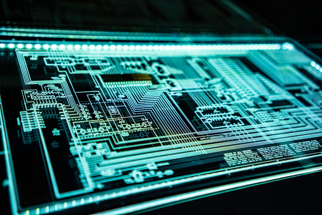
The main technical challenges associated with packaging of integrated photonic devices are the sub-micron dimensions and high tolerances needed to assemble components, particularly components such as optical fibres. For example, silicon waveguides have a typical cross-sectional area of 0.2 x 0.4 microns, approximately 50 times smaller than the core of a standard optical fibre. This presents a major packaging challenge, and requires the use of special mode-adaptors to taper-down the larger optical field from the fibre to the smaller waveguide. Mode-adaptors can be developed for edge or surface coupling to integrated photonic waveguides. However, mode-adaptors require specialised processing steps, often outside the capabilities of standard foundry processes. Furthermore, the alignment of fibre to waveguide requires the use of high precision packaging equipment using active alignment processes, where the coupled optical power is continuously monitored during the packaging process. This results in a slow process, limiting the throughput of packaged devices. Integrated photonics holds the potential to address mass markets in areas such as datacoms and disposable medical diagnostics, and the throughput limitation and associated high cost of packaging presents a major roadblock to addressing these emerging markets. New (non-active) packaging techniques and materials are under development to address these challenges, including innovative fast flipchip packaging processes and narrow core high NA optical fibre which is better matched to the dimensions of the small photonic waveguides. The combination of innovative PIC designs, new optical materials, and more advanced packaging equipment and processes is starting to make an impact on the cost and throughput issues.
What technology can be borrowed from mainstream electronics and where does the PIC community need to find new solutions?
Electronic packaging technologies provide excellent high throughput capabilities, but typically have poorer alignment tolerance than the sub-micron tolerances needed for optical packaging. To overcome this issue, coupling structures on PIC devices need to be modified to enable more relaxed alignment tolerances. Improved mode-adaptors which can provide more relaxed alignment tolerances are needed, as this enables packaging equipment providers to use conventional electronic assembly technologies, such as fast flipchip assembly on optical interposers or motherboards. To achieve this, packaging equipment providers and PIC designers need to work more closely (to-date there has been little or no collaboration between them). More relaxed alignment tolerances may result in lower coupling efficiencies, but the trade-off in faster (and lower cost) packaging processes may be acceptable for certain applications (eg. biomedical sensing where transmission distances are very short and power budgets are less demanding). Electronic packaging processes such as flipchip assembly also enable wafer-scale packaging rather than device-by-device processes. Moving towards more wafer-scale packaging, using the know-how gained from electronic packaging technologies, will drive significant cost reduction and greatly increase throughput.
Solving the current pinch points in packaging PIC devices will benefit the community as a whole, so in many cases it makes sense for stakeholders to team up. Can you tell us about how your Tyndall group is partnering with other key players to drive solutions in this area?
Tyndall has been taking a lead in developing PIC packaging design rules, which lead to the development of PIC packaging standards. To-date, there have been no design rules available to guide PIC designers to ensure their devices are suitably designed for packaging. In collaboration with PIC foundries such as IMEC, we have started to generate packaging design rules to account for optical and electronic packaging. As a result, PIC designers can follow these rules during the PIC layout stage of the process, making it much easier for us to package their devices. Furthermore, we have started to collaborate with the PIC software design companies such as PhoeniX and Luceda Photonics, incorporating our design rules into their software much like what is already available for electronic IC design. The next step is for us to increase collaborations with other PIC foundries to ensure all PIC designers take account of these packaging design rules. We are also starting to work with the equipment providers, ensuring the tools on their equipment are compatible with PIC packaging materials, such as optical fibres and micro optics. Standardisation of equipment is also an important factor to ensure more cost effective packaging processes. We see collaboration along the complete PIC supply chain as critical to ensuring more cost-effective and sustainable packaging processes.
Photonic devices have long been a part of the telecoms industry and there's growing excitement about PIC deployment in data centres. How do you see the applications landscape evolving? And what other areas will benefit as packaging expertise evolves and the technology becomes more accessible to other communities?
Data centres are definitely driving the demand for PIC technologies. Other markets where we see great opportunities are in sensing and medical diagnostics. For example, we are seeing companies replace bulky free space optical systems with much more compact integrated photonic solutions for sensing applications. Applications such as distributed Bragg fibre sensing are using integrated photonic interrogators in applications where performance, weight and size are critical parameters (eg. mechanical stress sensing in aircraft). Another emerging market where integrated photonics is beginning to make a big impact is point-of-care medical diagnostics, which is a truly mass market. Applications such as glucose monitoring for diabetic patients utilises the sensing capabilities of integrated photonic waveguides and can be implemented in patient implantable or wearable form. As with datacoms, these applications require the integration of light sources on the PIC platform, or remotely couple light to the PIC using free space optics and off-chip light sources. The latter approach is attractive as it enables highly cost-effective disposable PIC based sensors. Another feature of these medical devices is the integration of microfluidic components which are used to deliver the sample for analysis to the PIC platform. These are all packaging related challenges, and know-how gained in developing solutions for datacom applications is being re-used to address challenges in these emerging application areas "“ we see a strong cross-over between packaging technologies developed for communications and sensing-diagnostics.
Biography
Peter O'Brien received his PhD in physics from University College Cork (Ireland) in 1999, and was a postdoctoral scholar at the California Institute of Technology and NASA's Jet Propulsion Laboratory. His business expertise includes founding two photonic companies, the second of which he grew from start-up to a successful company sale in 5 years (2004-09), as well as industrial experience as manager of a large silicon fabrication facility and advisor to a number of venture capital companies, with a focus on investments in photonic start-up companies. Peter went on to establish the Photonics Packaging and Integration Group at the Tyndall Institute, Ireland, which has become a leader in providing advanced photonic packaging solutions to industry. His team partners in multiple EU (FP7 and H2020) projects, where it takes the lead role in packaging activities. The packaging group also participates in the PIX4LIFE Pilot Line, and is a partner of the ACTPHAST consortium (www.actphast.eu). In addition, Peter is deputy director of the Irish Photonics Integration Centre, a EURO 30 million investment by the Irish government in the area of integrated photonics.
Device development: Tyndall's Photonics Packaging and Integration Group at work in the lab