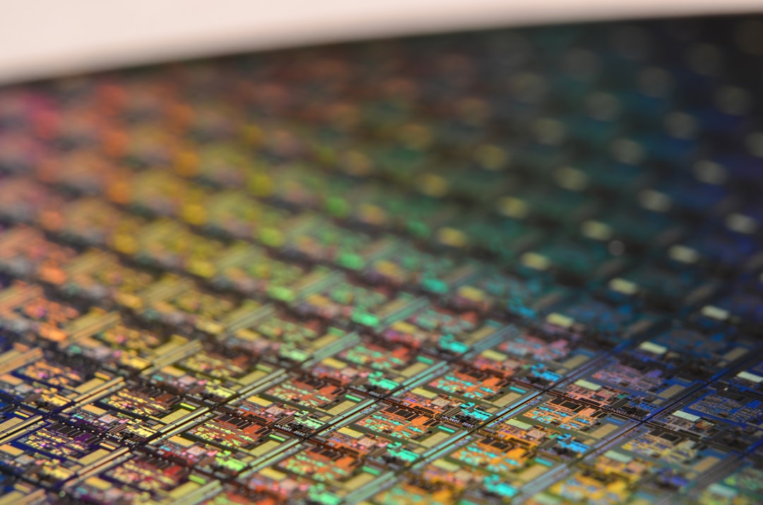
In the lab: uniting lasers and photodetectors in GaN

Integrating multiple functions on the same chip paves the way for advancing a range of applications, including smart lighting, displays and visible light communication. PIC International's sister title -- Compound Semiconductor magazine -- reports on a collaboration between KAUST, UCSB and KACST that's making headway by bringing together a III"“nitride waveguide photodetector with a laser diode emitting at 405 nm.
A collaboration between researchers in the US and Saudi Arabia has integrated a GaN laser and photodetector on the same chip, to create a device that offers optical power monitoring and on-chip communication.
The team believes that their device is the first to operate in the visible spectrum and deliver photonic integration via the use of the same InGaN/GaN quantum-well active region.
"Such a device is important for achieving a feedback loop to enable constant luminous lighting and realising high date rate, visible light communication systems "“ a step towards high-quality, smart lighting," argues corresponding author Boon Ooi from King Abdullah University of Science and Technology.
One of the merits of the work is that it avoids the strong internal electric field on the c-plane, which causes a large separation between the absorption and emission peaks. The approach of Ooi's group, working with researchers at the University of California, Santa Barbara, and King Abdulaziz City for Science and Technology, is to fabricate their photonic chip on the semi-polar plane of GaN.
Their chip features a 505 mm-long, 405 nm laser. Near its rear facet, separated by 5 mm, is a 90 mm long waveguide photodiode. Between the laser and photodiode is an isolation trench, formed by focused ion beam milling. This allows the two devices to operate independently, thanks to an isolation resistance of about 1 MW.
Measurements from the front facet of the laser, which is operated continuously, reveal a threshold current of 130 mA and a slope efficiency of 0.4 W/A. This is in good agreement with measurements of the waveguide photodiode at zero bias, which show a significant increase in photocurrent when the laser diode's current is increased to 130 mA. At higher drive currents, lasing kicks in, and there is a significant increase in the photocurrent in the waveguide photodiode. This behaviour shows that the waveguide photodiode can be used for on-chip power monitoring.
Biasing the photodiode leads to enhanced optical responsivity. When driving the laser with 5 ms pulses at a 10 percent duty cycle to minimise heating, an increase in the bias from 0 V to 10 V leads to an increase in responsivity "“ the ratio of the photocurrent to the incident optical power "“ from 0.0018 A/W to 0.051 A/W. According to the team, this figure of merit is far higher than that for equivalent photodiodes on the c-plane, which have a responsivity of 0.001 A/W to 0.01 A/W.
Frequency measurements on the waveguide photodiode indicate a 3 dB bandwidth of 230 MHz. This is vastly superior to GaN Schottky barrier photodiodes and p-i-n photodiodes, which have figures of 5.4 MHz and 10-20 MHz. Ooi attributes the far higher frequency of their waveguide photodiodes their small size, stemming from the narrow ridge design, and the higher responsivity in the semi-polar plane. The higher speed is claimed to showcase the potential of the chip as an integrated receiver for on-chip communication and visible light communication.
Even higher levels of performance should be possible. According to Ooi, the DC and high frequency photoresponse characteristics of the waveguide photodiode could be improved by optimising the design, including the form factor and the facet angle. "By reducing the junction capacitance to about 5 pF, a 3-dB bandwidth of more than 500 MHz is expected." Meanwhile, the efficiency of the laser could be increased by optimising the facet and turning to high-quality high-reflection coatings.
Plans for the future include the development of a multiple-section integration technology. This could enable complex monolithic on-chip integration of III-N light emitters and receivers for smart lighting, displays, and visible light communication.
Adding more functionalities could lead to photonic integrated circuits for optical switching, clocking and optical interconnects.Integrating a GaN laser and waveguide photodetector could aid smart lighting, by allowing the monitoring of optical power.